Method for forming metal wiring groove

A metal wiring and trench technology, applied in the field of semiconductor manufacturing, can solve the problems of critical size gap, performance degradation of semiconductor devices, and difficulty in controlling the etching size, so as to achieve the effect of improving performance and easing the etching rate

Active Publication Date: 2011-01-26
SEMICON MFG INT (SHANGHAI) CORP +1
View PDF1 Cites 1 Cited by
  • Summary
  • Abstract
  • Description
  • Claims
  • Application Information

AI Technical Summary

Problems solved by technology

[0007] When using the mixed gas of carbon tetrafluoride, oxygen and argon in the prior art to etch the bottom anti-reflection layer, it is difficult to control the etching size, and the critical dimension of the second groove pattern formed in the bottom anti-reflection layer Usually greater than the predetermined value, there will be a gap between the critical dimension of the subsequently formed metal wiring trench and the predetermined value, resulting in a decrease in the performance of the semiconductor device

Method used


Image

  • Method for forming metal wiring groove
  • Method for forming metal wiring groove
  • Method for forming metal wiring groove

Examples


Embodiment Construction

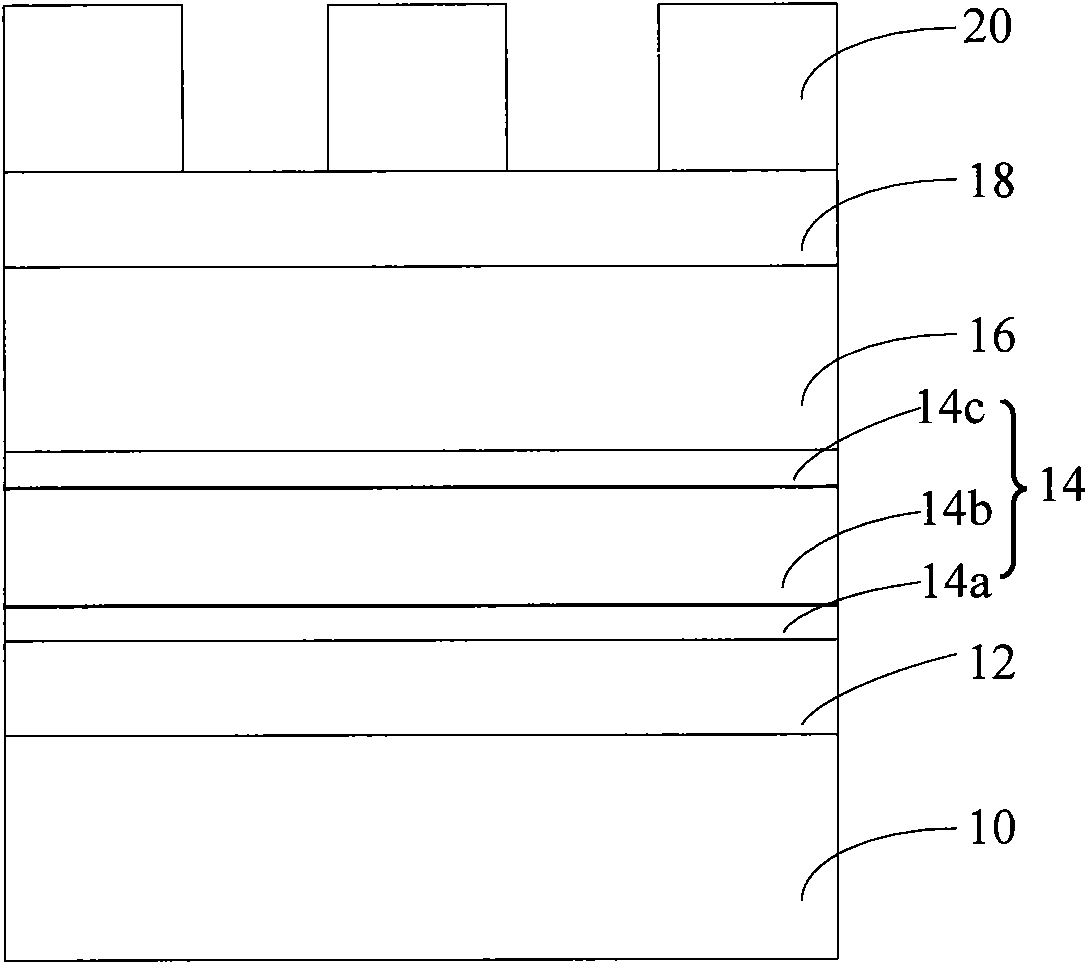
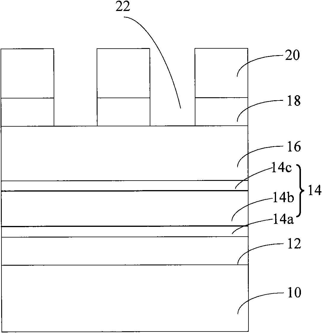
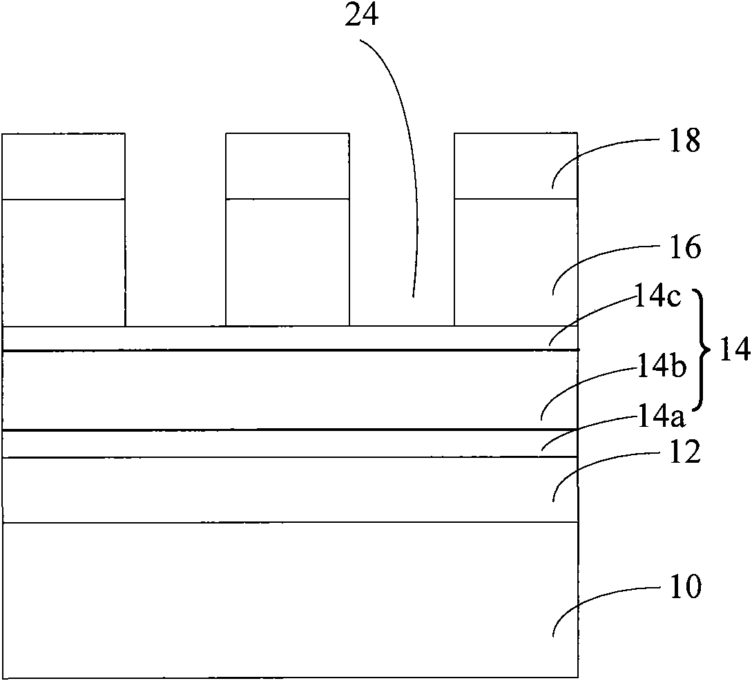
[0018] In the present invention, the process flow of performing an etching process to form metal wiring grooves in the process of forming metal wiring is as follows: step S11 is performed to provide a semiconductor substrate, and an interlayer dielectric layer, a dielectric layer, and a semiconductor substrate are sequentially formed on the semiconductor substrate. Bottom anti-reflective layer, low temperature silicon oxide layer and patterned photoresist layer.

[0019] The material of the interlayer dielectric layer is silicon oxide or silicon oxynitride, which is used for isolation between semiconductor devices.

[0020] The dielectric layer includes a silicon carbonitride layer with a thickness of 300 angstroms, a low dielectric constant dielectric layer with a thickness of 1550 angstroms, and a silicon oxide protection layer with a thickness of 500 angstroms, which are sequentially located on the interlayer dielectric layer.

[0021] The bottom antireflection layer has a ...


PUM

PropertyMeasurementUnit
thicknessaaaaaaaaaa
thicknessaaaaaaaaaa
thicknessaaaaaaaaaa

Abstract

The invention relates to a method for forming a metal wiring groove, which comprises the following steps: providing a semiconductor substrate; sequentially forming an interlayer medium layer, a dielectric layer, a bottom antireflection layer, a low-temperature silicon oxide layer and a patterning photoresist layer on the semiconductor substrate; taking the patterning photoresist layer as a mask, and etching the low-temperature silicon oxide layer to expose the bottom antireflection layer to form a first groove pattern; taking the patterning photoresist layer and the low-temperature silicon oxide layer as masks, and etching the bottom antireflection layer along the first groove pattern to expose the dielectric layer to form a second groove pattern, wherein the etching gas is mixed gas of carbon dioxide and carbon monoxide; and taking the low-temperature silicon oxide layer and the antireflection layer as masks, and etching the dielectric layer along the second groove pattern to form the metal wiring groove. The invention can effectively control the critical dimension of the second groove pattern formed on the bottom antireflection layer to achieve a predetermined value, so that thecritical dimension of the sequentially formed metal wiring groove is the same as a predetermined value, and the performance of a semiconductor device is improved.

Description

technical field [0001] The invention relates to the technical field of semiconductor manufacturing, in particular to a method for forming metal wiring grooves. Background technique [0002] Generally, the semiconductor process is to use deposition process, photolithography process, etching process, etc. to form integrated circuit devices on silicon wafers. In order to connect various components to form an integrated circuit, a relatively high-conductivity metal material such as copper is usually used for wiring, that is, metal wiring. The structure used to connect circuits between semiconductor devices is generally a metal wiring trench structure, for example, the method for forming trench plugs in a metal wiring structure provided by Chinese patent application document CN98118290. [0003] In the post-production process of semiconductor devices, the etching process before the metal wiring process is as follows: Figure 1 to Figure 4 shown. refer to figure 1 A semiconduc...

Claims


Application Information

Patent Timeline
Patent Type & Authority Applications(China)
IPC IPC(8): H01L21/768H01L21/311
Inventor 李凡洪中山
Owner SEMICON MFG INT (SHANGHAI) CORP
Why Eureka
Try Eureka