Wafer structure and manufacturing method thereof

A manufacturing method and wafer technology, which can be used in semiconductor/solid-state device manufacturing, electrical components, electrical solid-state devices, etc., can solve problems such as limiting the development breadth of semiconductors, and achieve the effect of simple process manufacturing

Inactive Publication Date: 2011-01-26
SHANGHAI HUAHONG GRACE SEMICON MFG CORP
View PDF7 Cites 0 Cited by
  • Summary
  • Abstract
  • Description
  • Claims
  • Application Information

AI Technical Summary

Problems solved by technology

The process of manufacturing multiple integrated circuits on a wafer is very mature, but in addition, there is no way to integrate other functions on the same wafer, which limits the breadth of semiconductor development

Method used


Image

  • Wafer structure and manufacturing method thereof
  • Wafer structure and manufacturing method thereof
  • Wafer structure and manufacturing method thereof

Examples


Embodiment Construction

[0022] The specific implementation manners of the present invention will be described in further detail below with reference to the accompanying drawings. Throughout the description, like reference numerals refer to like parts.

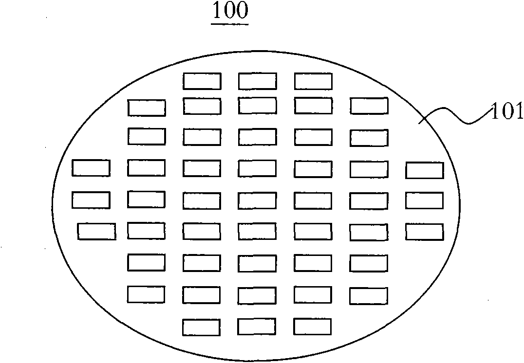
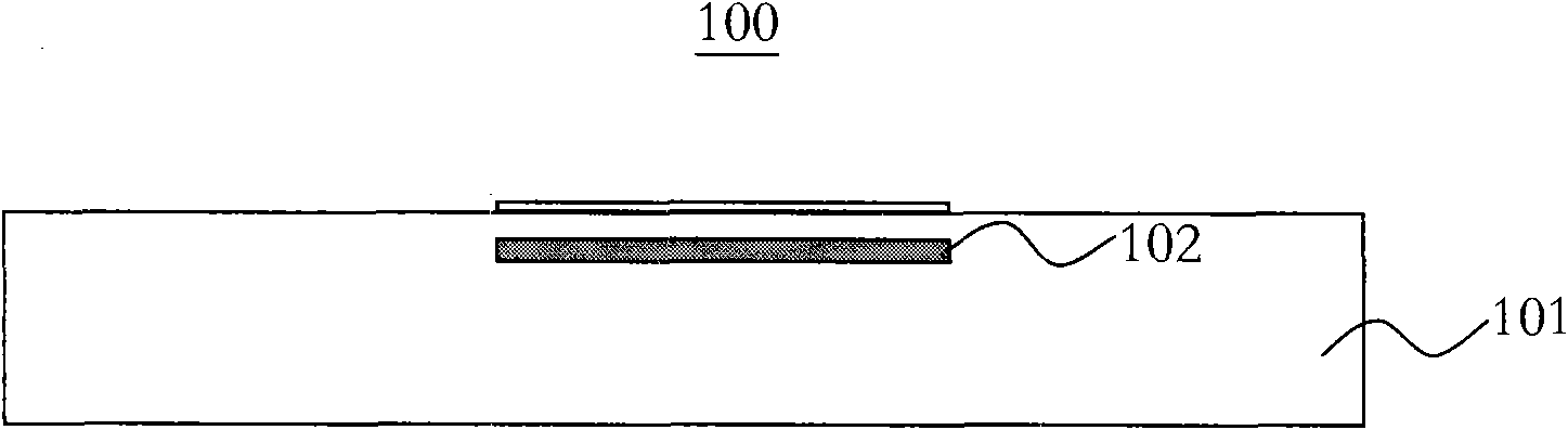
[0023] In the wafer structure and the manufacturing method of the wafer structure of the present invention, not only the substrate for manufacturing electrical devices but also the substrate for manufacturing optical devices is integrated on the wafer, realizing the integration of optoelectronic integrated components. In the manufacturing process of the wafer, the combination of the semiconductor substrate on the buried oxide layer and the semiconductor substrate not embedded in the buried oxide layer is distributed on the wafer, the process is simple and efficient, and it is beneficial to the later cutting process.

[0024] Figure 1a is a schematic top view of the wafer structure. Figure 1b is a schematic cross-sectional view of the wafer structur...


PUM


Abstract

The invention provides a wafer structure comprising a semiconductor substrate embedded with a plurality of buried oxide layers, wherein the buried oxide layers are breadthwise generated in the semiconductor substrate at intervals. The invention also provides a manufacturing method of the wafer structure, comprising: injecting oxygen ions in the surface of a wafer; generating the buried oxide layers in a semiconductor substrate required to be oxidized; forming the base plate of an electrical appliance by the semiconductor substrate which is not embedded into the buried oxide layers; and forming the base plate of an optical device by the semiconductor substrate which is positioned above the buried oxide layers. The wafer is provided with the base plate capable of manufacturing the electrical appliances, and is integrated with the base plate for manufacturing the optical device so as to realize the integration of integrated optoelectronic elements.

Description

technical field [0001] The invention relates to the technical field of semiconductor devices, in particular to a wafer preparation process. Background technique [0002] At present, chips are widely used in various modern electronic devices such as liquid crystal display devices, mobile phones, and personal digital assistants due to their high integration, low power consumption, and small size. [0003] Typically, a chip is obtained through the following manufacturing process: first, a wafer with multiple integrated circuits is formed; then, each integrated circuit of the wafer is tested; finally, each integrated circuit is diced from the wafer to produce into chips. Existing wafers with multiple integrated circuits are mostly used as substrates for electrical devices, electronic devices that use the special electrical properties of semiconductor materials to complete specific functions, and can be used as rectifiers, oscillators, amplifiers and other equipment. The proces...

Claims


Application Information

Patent Timeline
Patent Type & Authority Applications(China)
IPC IPC(8): H01L27/00H01L21/762
Inventor 仇超
Owner SHANGHAI HUAHONG GRACE SEMICON MFG CORP
Why Eureka
Try Eureka