High-precision band-gap reference source circuit based on emitter current compensation
A technology of emitter current and compensation circuit, which is applied in the direction of adjusting electrical variables, control/regulation systems, instruments, etc., to achieve the effects of reducing influence, achieving compatibility, and simple structure
- Summary
- Abstract
- Description
- Claims
- Application Information
AI Technical Summary
Problems solved by technology
Method used
Image
Examples
Embodiment Construction
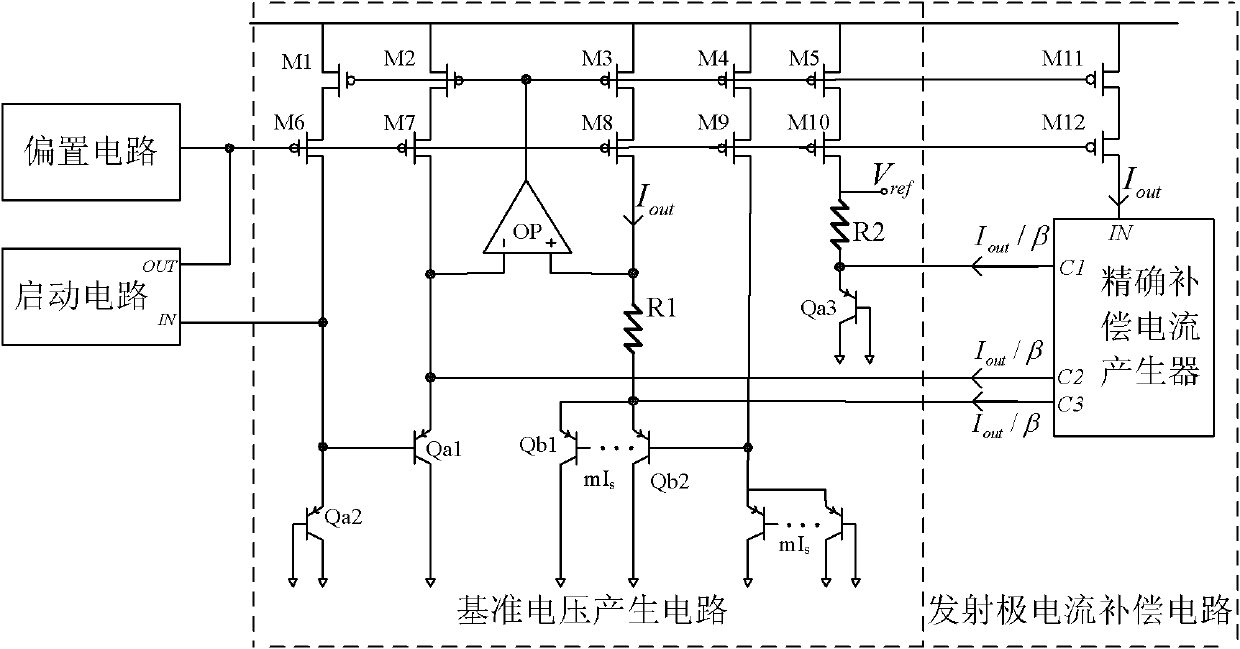
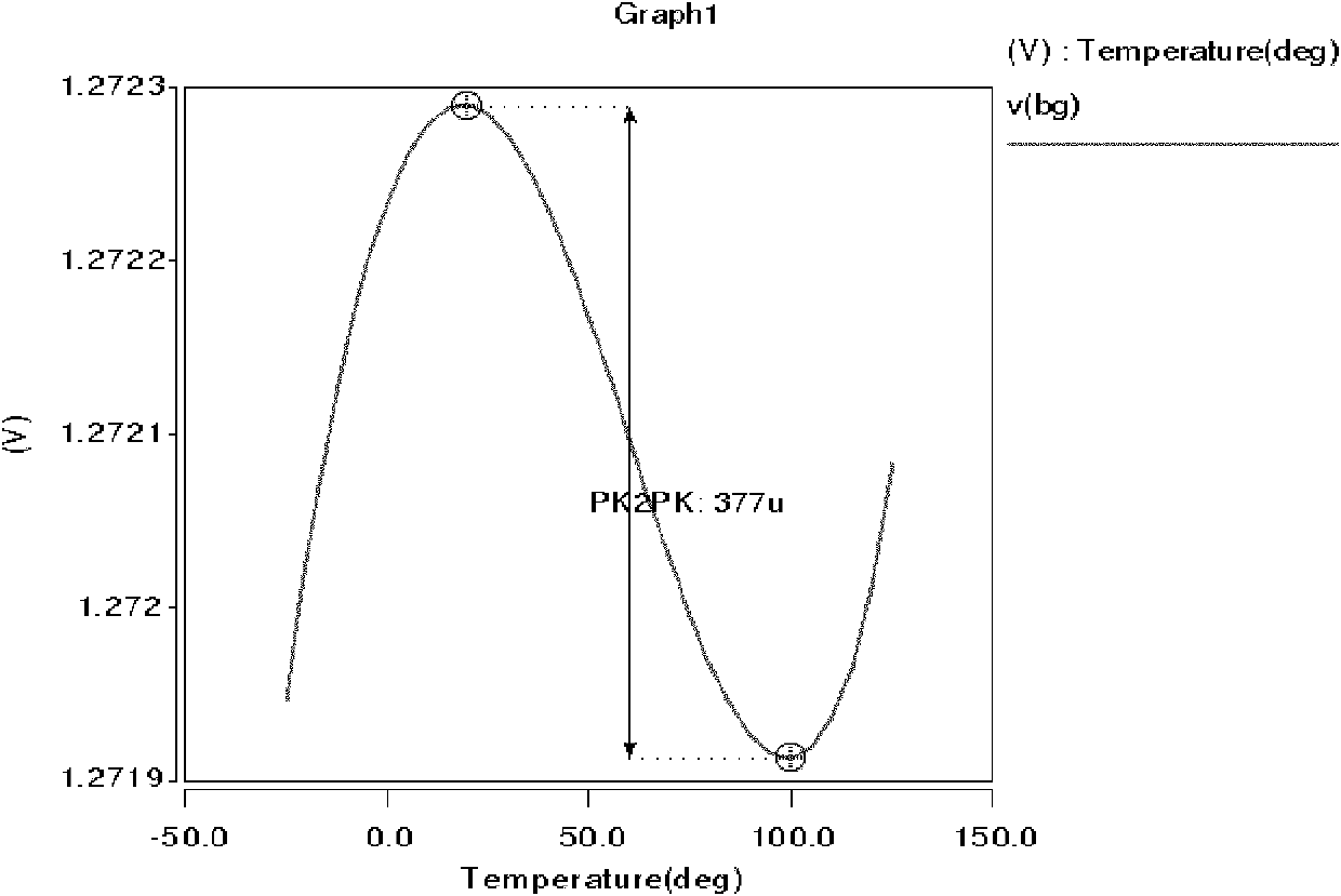
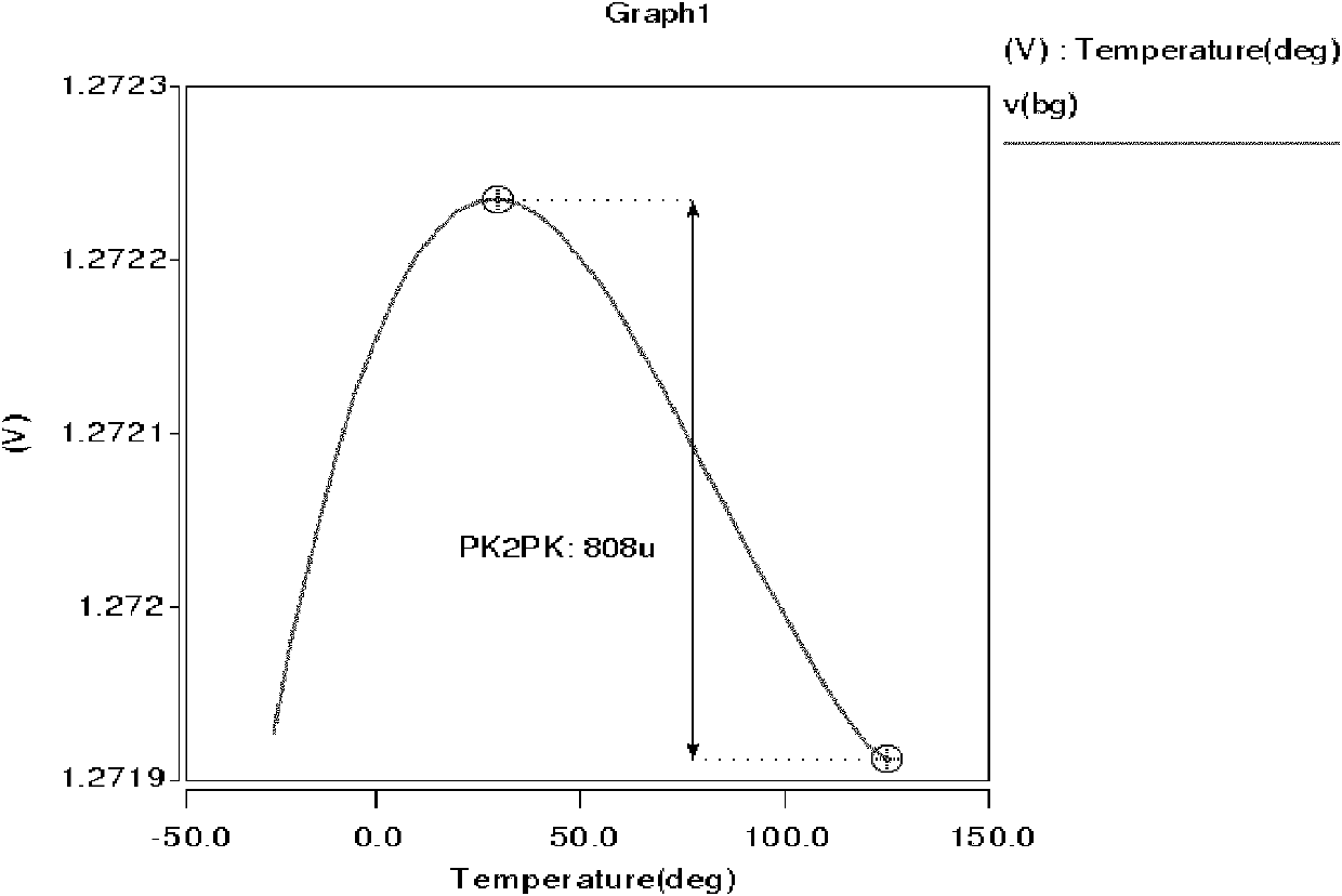
[0015] like figure 1 As shown, the circuit of the present invention can be divided into four parts: a start-up circuit, a bias circuit, a reference voltage generating circuit, and an emitter current compensation circuit. The function of the bias circuit is to provide gate bias voltage for the cascode transistors M1~M5 and M12 in the reference voltage generation circuit and the emitter current compensation circuit, so that they can work in the saturation region and improve the output impedance of the cascode transistors. , to enhance its ability to resist power interference. The reference voltage generation circuit is composed of PMOS transistors M1~M10, operational amplifier OP, resistors R1, R2, transistors Qa1, Qa2, Qa3, Qb1 and Qb2. Adding a cascode current mirror can increase the accuracy of the reference current source and effectively Increases the current source's ability to withstand voltage changes. But a problem with this circuit is the possibility of a deadlock sta...
PUM
 Abstract
Description
Claims
Application Information


