

Semiconductor-based large-area flexible electronic devices
A technology of electronic devices and semiconductors, applied in the field of large-area flexible electronic devices based on semiconductors
- Summary
- Abstract
- Description
- Claims
- Application Information
AI Technical Summary
Problems solved by technology
Method used
Image

Examples
Embodiment 1
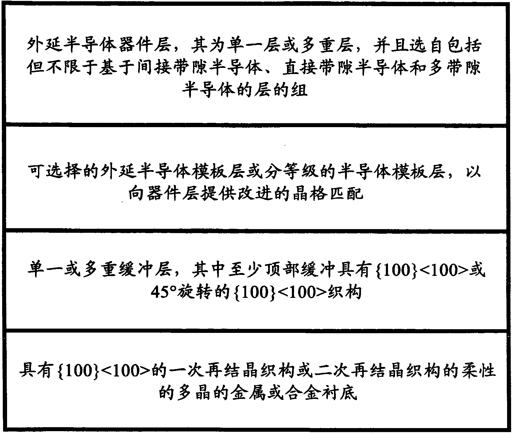
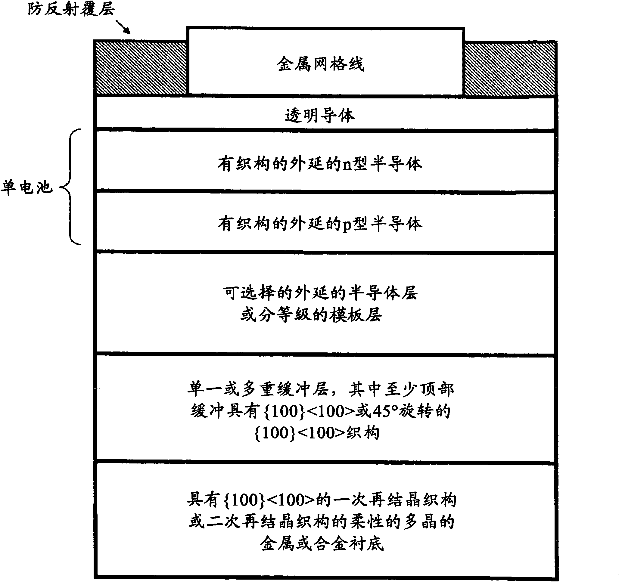
[0097] Example 1: [100] uniaxially textured metal substrates were prepared by sequentially pressing or forging cubic metals or alloys by compression to large total deformation and then recrystallization annealing. For example, a NiW alloy with 3-9 at% W is used, compressed to 90% deformation by uniaxial extrusion, and then annealed in a furnace at a temperature above the primary recrystallization temperature of the alloy. The formed primary recrystallization texture is [100] texture. By raising the annealing temperature to high temperatures close to 1000°C, an average grain size greater than 100 µm is formed. An epitaxial buffer layer is then deposited on the substrate. For example, chemical vapor deposition (CVD) is used to deposit epitaxial TiN layers at deposition temperatures in the range of 300°C to 600°C. An epitaxial Si layer is then deposited using a CVD-type process at a deposition temperature in the range of 300°C to 900°C. This results in the formation of a [100]...
Embodiment 2
[0098] Example 2: [110] uniaxially textured metal substrates were prepared by sequentially pressing cubic metals or alloys by compression to large total deformation and then recrystallization annealing. For example, a NiW alloy with 3-9 at% W is used, compressed to 90% deformation by uniaxial extrusion, and then annealed in a furnace at a temperature above the primary recrystallization temperature of the alloy. The primary recrystallization texture formed is [110] texture. By raising the annealing temperature to high temperatures close to 1000°C, an average grain size greater than 100 µm is formed. An epitaxial buffer layer is then deposited on the substrate. For example, chemical vapor deposition (CVD) is used to deposit epitaxial TiN layers at deposition temperatures in the range of 300°C to 600°C. An epitaxial Si layer is then deposited using a CVD-type process at a deposition temperature in the range of 300°C to 900°C. This results in the formation of a [110] uniaxially...
Embodiment 3
[0099] Example 3: Figure 10 shows a crystallographically textured, flexible NiW alloy in cross-section with a textured Si semiconductor layer above the alloy and an epitaxial buffer layer of textured TiN in between. An idealized schematic diagram of . This device and figure 1 A and B depict identical devices. [100] textured biaxially textured Ni-3at%W was prepared by continuous rolling of a powder metallurgically derived alloy coil from a thickness of about 120 mils to a foil thickness of about 2 mils or 50 microns. The as-rolled crystallographic texture of the foil or strip is the standard Cu-type rolled texture of greatly deformed FCC metals. After the strip is degreased and dried, the strip is loaded into a reel-to-reel high vacuum (10 -8 entrust) in the room. Strips in ~3×10 -7 Torr of hydrogen sulfide gas is pulled through the hot zone of the furnace at such a rate that each part is heated to 1250°C within twenty minutes to form sulfur c(2×2) super structure. Aft...
PUM
| Property | Measurement | Unit |
|---|---|---|
| Average grain size | aaaaa | aaaaa |
| Rotation angle | aaaaa | aaaaa |
| Diameter | aaaaa | aaaaa |
Abstract
Description
Claims
Application Information