Circuit board

A technology of circuit board and conductive paste, which is applied in the direction of printed circuit, printed circuit, circuit device, etc., can solve the problems of poor accuracy of the area, contamination, leakage, etc., and achieve the goal of eliminating deviation, large line width, and increasing accuracy Effect

Inactive Publication Date: 2011-02-23
SUMITOMO BAKELITE CO LTD
View PDF0 Cites 3 Cited by
  • Summary
  • Abstract
  • Description
  • Claims
  • Application Information

AI Technical Summary

Problems solved by technology

[0015] Although, in order to obtain the ideal Z 0 , it is possible to form a ground plane with voids (for example, in the shape of a mesh) by printing with the paste as described above, but there will be a problem that the accuracy of the area will be deteriorated due to printing, and it will often suffer greatly. Fouling, leakage (bleeding) and other effects
[0016] In addition, for the latter, that is, for the shielding film on which a metal layer is formed as a film by vacuum deposition or the like, unless an impractical microhole punching process unsuitable for mass production is performed, it cannot be formed with voids. (e.g. mesh-shaped) ground plane

Method used


Image

  • Circuit board
  • Circuit board
  • Circuit board

Examples


Embodiment Construction

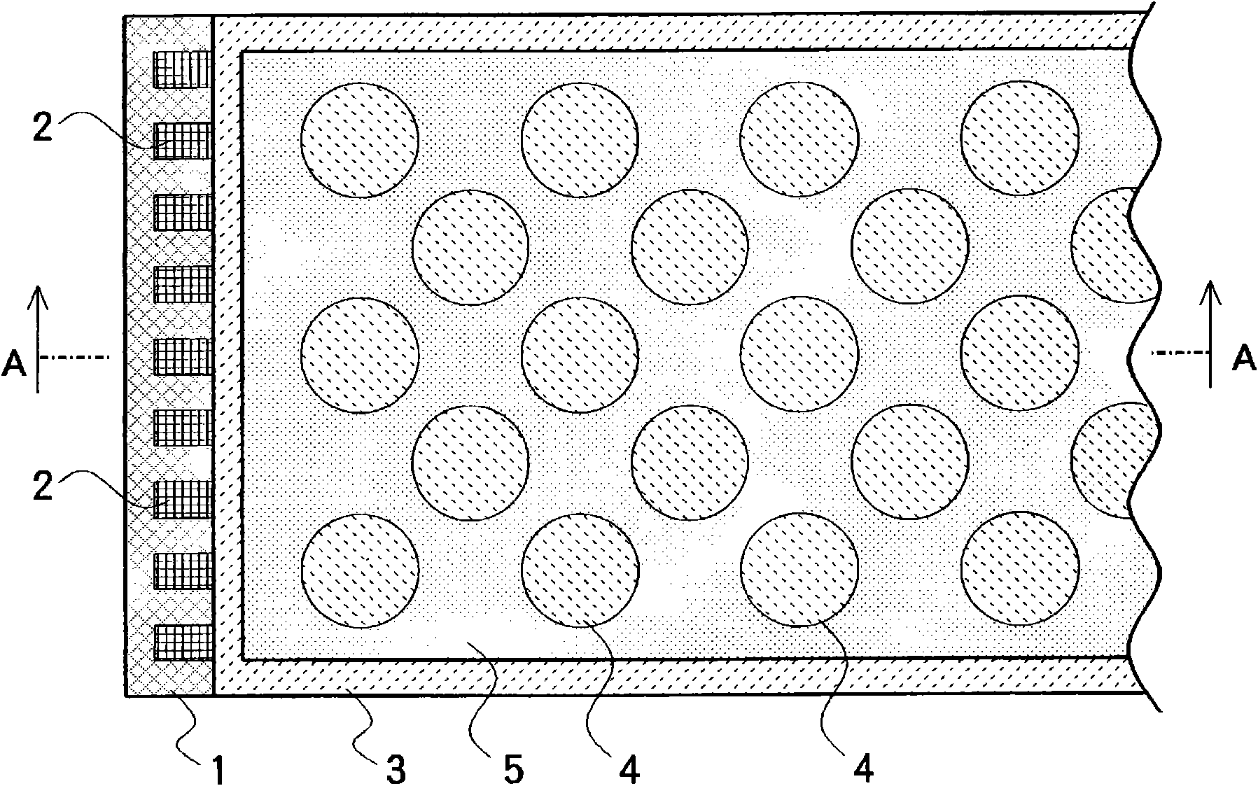
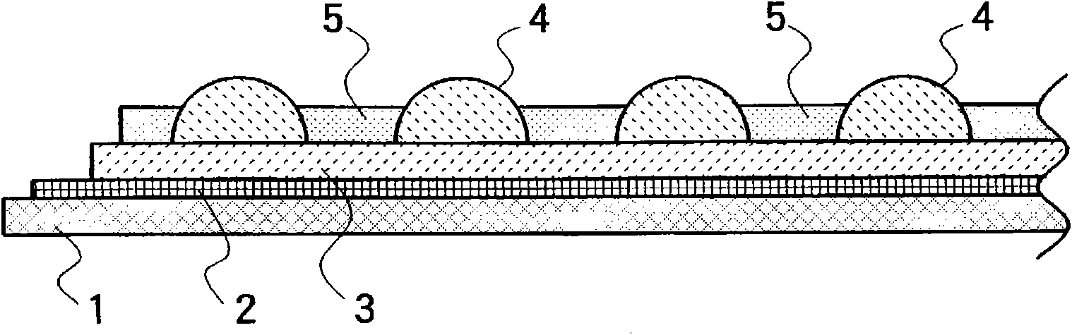
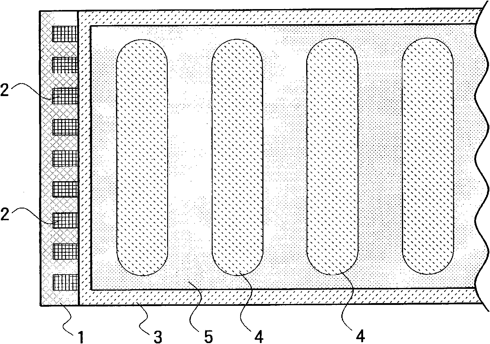
[0046] figure 1 with figure 2 is a schematic diagram showing a first preferred embodiment in which a circuit board according to the present invention is applied to a flexible printed circuit board, figure 1 shows the floor plan of the board, figure 2 along figure 1 The arrow direction of the A-A line in the figure shows the circuit board in a cross-sectional view.

[0047] figure 1 with figure 2 The reference numeral 1 in represents a film-shaped base substrate formed of an insulating material, and a plurality of signal lines 2 formed of copper foil are arranged on one surface of the base substrate 1 ( figure 2 upper surface shown). Furthermore, an insulating layer 3 is stacked to the base substrate 1 so as to cover the above-mentioned signal line 2 .

[0048] For example, a polyester film, a polyimide film, a liquid crystal polymer film, or the like can be used as the above-mentioned base substrate 1 . Among these films, polyimide film is ideal because it has high...


PUM

PropertyMeasurementUnit
thicknessaaaaaaaaaa

Abstract

Signal wiring (2) is formed on one side of a base material (1), and a coverlay film (3) is laminated thereon. A plurality of protrusions (4) formed of an insulating material are formed on the upper surface of the coverlay film at a substantially constant interval in the length and breadth direction, and a ground layer (5) formed of silver paste, for example, is formed on the coverlay film excepting the positions where the protrusions are arranged. Since the film of conductive paste is formed thinner than the thickness of the top of the protrusion formed on an insulating layer, substantially meshed openings (air gap portions) can be formed on the ground layer of conductive paste because of the existence of the protrusions. Consequently, a circuit board acting similarly to a ground plane having substantially meshed air gaps can be provided.

Description

technical field [0001] The invention relates to a circuit board, in which a signal line is opposed to a ground layer through an insulating layer. Background technique [0002] For example, a circuit board on which a device operating in a high frequency band is mounted needs to make the characteristic impedance (hereinafter also referred to as Z) of a signal transmission line (hereinafter also referred to as a signal line) 0 ) is matched to the input-output impedance of the above device to suppress the reflection of the signal and suppress the generation of waveform distortion. [0003] As described above, in order to adjust the characteristic impedance of the signal transmission line, a strip structure or a microstrip structure is used, in which a signal transmission line (strip line) having an appropriate pattern width is connected to the ground through an insulating layer having an appropriate thickness. layer relative. [0004] The aforementioned ground plane in the afo...

Claims


Application Information

Patent Timeline
Patent Type & Authority Applications(China)
IPC IPC(8): H05K1/02H05K9/00
CPCH05K1/0224H05K1/095H05K1/0393H05K2201/09681H05K1/0253H05K2201/0715H05K3/4664H05K2201/09909
Inventor 及川昭
Owner SUMITOMO BAKELITE CO LTD
Why Eureka
Try Eureka