Unlock instant, AI-driven research and patent intelligence for your innovation.

Silicon-on-insulator waveguide grating coupler and manufacturing method thereof

A silicon-on-insulator and waveguide grating technology, which is applied in the coupling of optical waveguides, light guides, optics, etc., can solve the problems of device online testing and packaging difficulties, coupling efficiency reduction, chip performance limitations, etc.

Inactive Publication Date: 2011-03-02
INST OF SEMICONDUCTORS - CHINESE ACAD OF SCI
View PDF3 Cites 14 Cited by
  • Summary
  • Abstract
  • Description
  • Claims
  • Application Information

AI Technical Summary

Problems solved by technology

However, as the size of the silicon-on-insulator waveguide shrinks, the mode spot size of the light in the waveguide also becomes smaller than 1 μm, while the mode spot size in the optical fiber is 8-10 μm. The mismatch will lead to the appearance of radiation modes and back reflections. Light entering such a small-sized waveguide from an optical fiber often causes a large loss, which brings great difficulties to the on-line testing of the device and subsequent packaging. , the performance of the chip is also limited
Therefore, in the field of integrated optoelectronics, although silicon-on-insulator submicron waveguides can be used to make various highly integrated and high-performance optoelectronic devices, the coupling problem between optical waveguides and photonic devices for input and output light has always been a problem. a pressing issue
If the optical waveguide and grating coupler are prepared by one electron beam lithography and etching process by increasing the etching depth of the ordinary uniform periodic grating coupler, the coupling efficiency will be reduced.

Method used


Image

  • Silicon-on-insulator waveguide grating coupler and manufacturing method thereof
  • Silicon-on-insulator waveguide grating coupler and manufacturing method thereof
  • Silicon-on-insulator waveguide grating coupler and manufacturing method thereof

Examples


Embodiment Construction

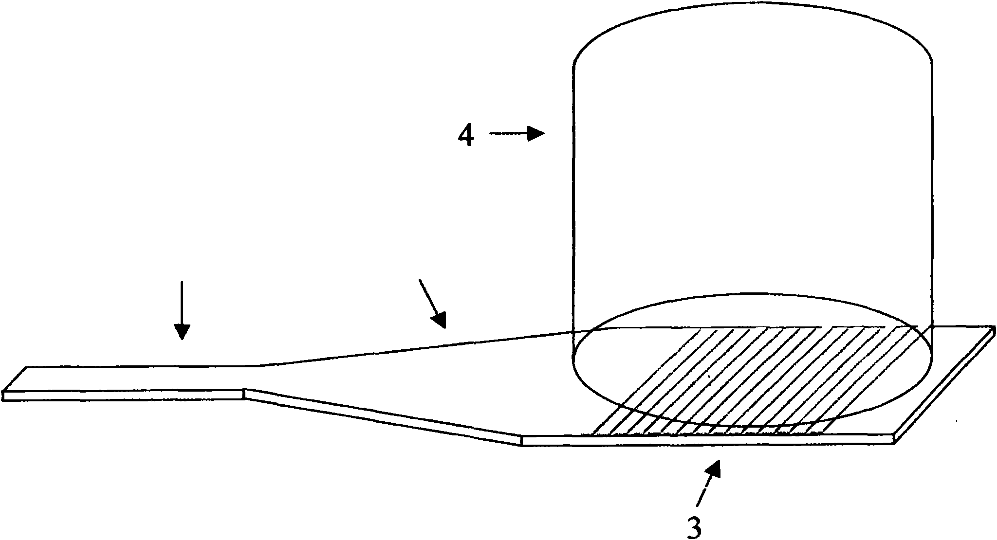
[0025] See figure 1 , figure 2 and image 3 As shown, the present invention provides a silicon-on-insulator waveguide grating coupler, the coupler adopts a silicon-on-insulator material, and includes:

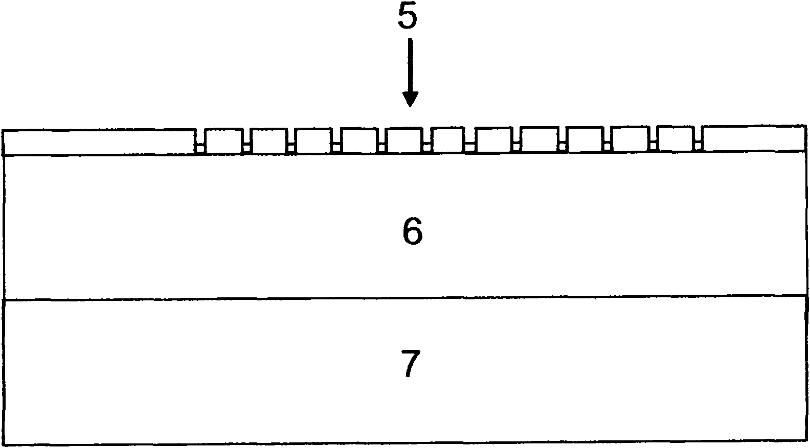
[0026] A substrate 7; the substrate is a silicon-on-insulator substrate, and the waveguide layer and the confinement layer are fabricated on the substrate.

[0027] A confinement layer 6, the confinement layer 6 is made on the substrate 7; the thickness of the confinement layer 6 is greater than 1 μm; the confinement layer is a silicon-on-insulator confinement layer, because its refractive index is smaller than the waveguide layer, it can confine light in the waveguide layer In the waveguide

[0028] A waveguide layer 5, the waveguide layer 5 is fabricated on the confinement layer 6, a diffraction grating 3 is fabricated laterally on one end of the waveguide layer 5, the thickness of the waveguide layer 5 is less than 1 μm; the waveguide layer 5 includes: submicron waveguide 1, Tape...


PUM

PropertyMeasurementUnit
Thicknessaaaaaaaaaa
Thicknessaaaaaaaaaa
Lengthaaaaaaaaaa

Abstract

The invention relates to a silicon-on-insulator waveguide grating coupler which adopts a silicon-on-insulator material, and comprises a substrate, a limiting layer, a waveguide layer and a photonic device, wherein the limiting layer is manufactured on the substrate; the waveguide layer is manufactured on the limiting layer; a diffraction grating is transversely manufactured at one end of the upper side of the waveguide layer; and a light emitting end or receiving end of the photonic device is arranged above the diffraction grating on the waveguide layer.

Description

Technical field [0001] The invention relates to the technical field of photonic devices, and is a grating waveguide coupler. The structure of the grating coupler can effectively reduce the coupling loss between optical fibers and submicron waveguides, and is easy to realize high-density optical device integration and on-chip testing of optical chips, and is widely used In optical communication, optical interconnection between chips, optical chip inspection and high-speed silicon electro-optical integration. Background technique [0002] Since the beginning of the new century, with the continuous development of micro-nano optoelectronic integration technology, the integration of chips has become higher and higher, the size of devices has been shrinking, and the waveguide used to transmit optical signals has gradually shrunk to the sub-micron scale. Among the many optical waveguide materials used in the communication band, the silicon-on-insulator material is easy to produce sub-mi...

Claims


Application Information

Patent Timeline
IPC IPC(8): G02B6/34G02B6/124G02B6/136
Inventor 周亮李智勇俞育德余金中
Owner INST OF SEMICONDUCTORS - CHINESE ACAD OF SCI
Features
  • R&D
  • Intellectual Property
  • Life Sciences
  • Materials
  • Tech Scout
  • Unparalleled Data Quality
  • Higher Quality Content
  • 60% Fewer Hallucinations
Learn More