Printed circuit board virtual manufacturing system of electronic design automation of electronic product and realization method thereof

A technology of virtual manufacturing system and electronic products, applied in computing, electrical digital data processing, special data processing applications, etc., can solve problems such as PCB board physical parameter errors, assemblability errors, etc., to save time and production costs, shorten The effect of reducing the manufacturing cycle and production cost

Inactive Publication Date: 2011-03-16
CHANGZHOU AUTOSMT INFORMATION TECH
View PDF3 Cites 36 Cited by
  • Summary
  • Abstract
  • Description
  • Claims
  • Application Information

AI Technical Summary

Problems solved by technology

At present, various EDA design conversion technologies and error checking technologies are being developed at home and abroad, but 3D visualization cannot directly display the layout of EDA-designed PCB boards and the PCB situation afte

Method used


Image

  • Printed circuit board virtual manufacturing system of electronic design automation of electronic product and realization method thereof
  • Printed circuit board virtual manufacturing system of electronic design automation of electronic product and realization method thereof
  • Printed circuit board virtual manufacturing system of electronic design automation of electronic product and realization method thereof

Examples


Embodiment Construction

[0021] The present invention will now be described in further detail in conjunction with the accompanying drawings and preferred embodiments. These drawings are all simplified schematic diagrams, which only illustrate the basic structure of the present invention in a schematic manner, so they only show the configurations related to the present invention.

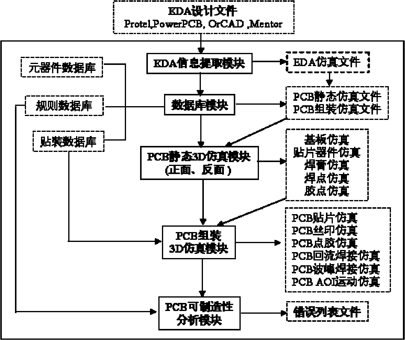
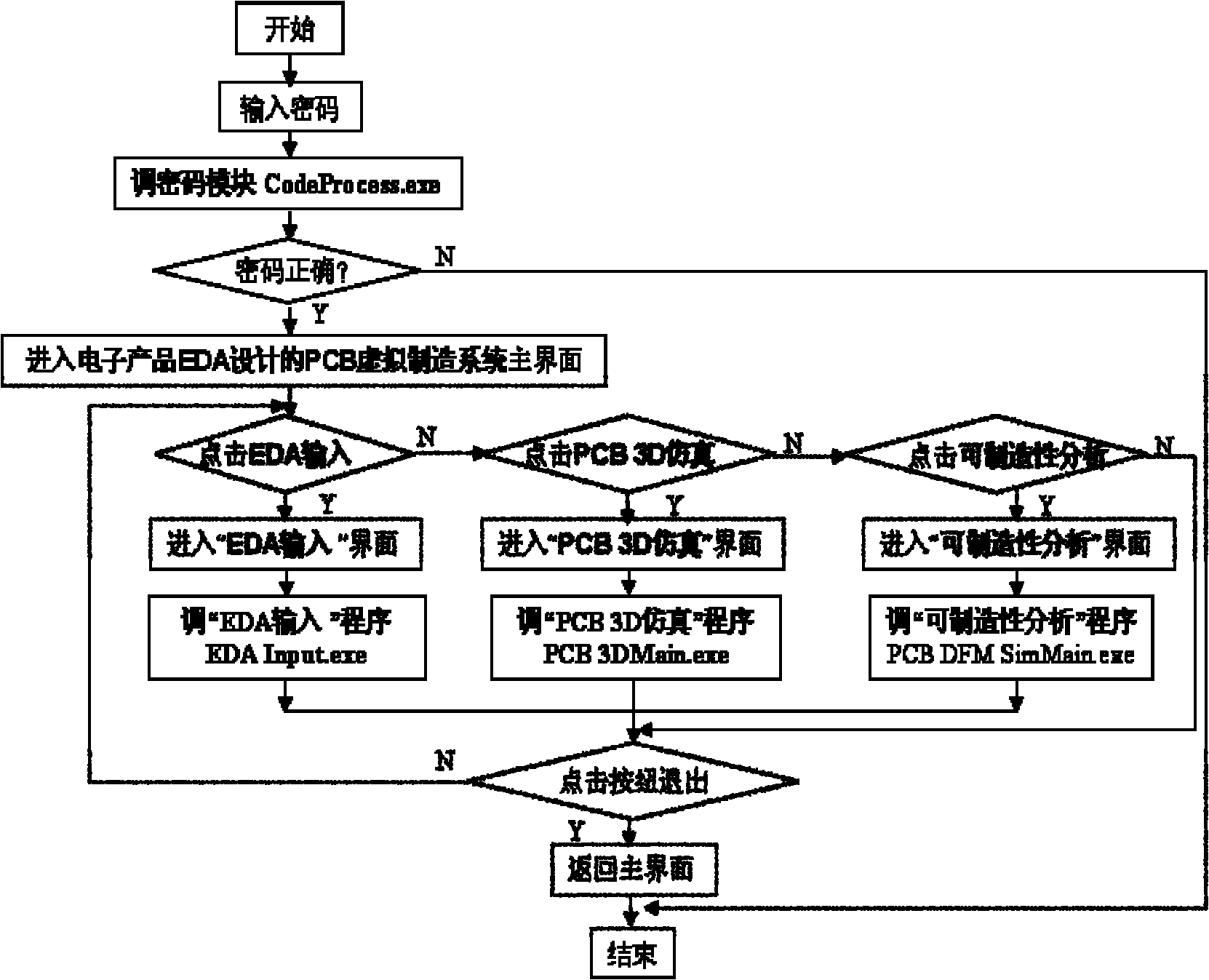
[0022] This embodiment is a kind of PCB virtual manufacturing system designed by electronic product EDA, such as figure 1 The system structure shown includes:

[0023] 1) EDA information extraction module: read in the EDA design file, extract the information and discrimination parameters of PCB board design from it, save it as a Chinese EDA simulation file in a unified format, and input the data into the database;

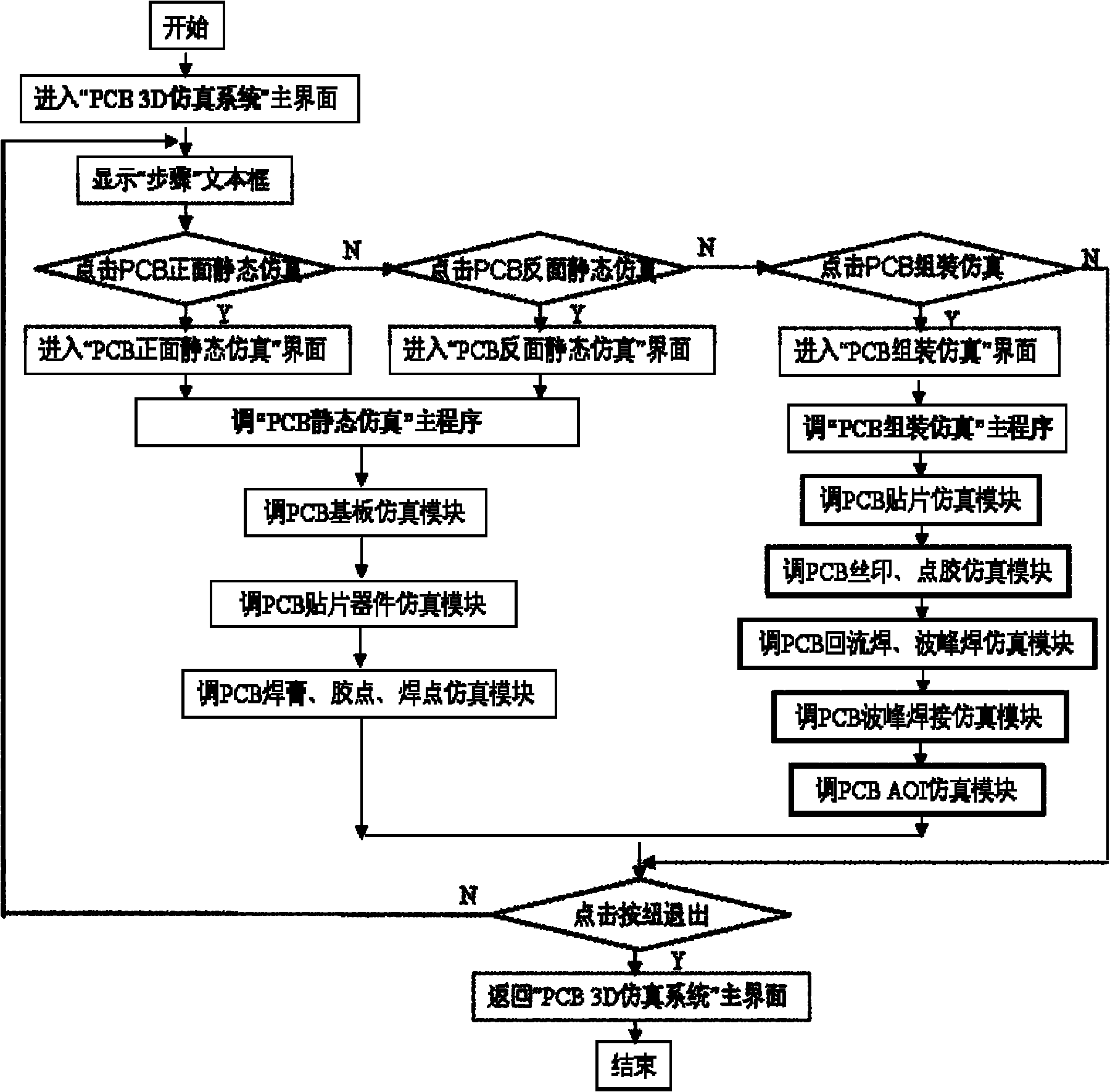
[0024] 2) PCB static and assembly 3D simulation module: According to the simulation information extracted from the EDA information extraction module, the simulation model of the virtual manufacturing system is e...


PUM


Abstract

The invention relates to a printed circuit board (PCB) virtual manufacturing system of the electronic design automation (EDA) of the electronic product and a realization method thereof. The realization method comprises the following steps: all types of EDA design files can be extracted and converted to an EDA simulation file with the same format and data are input in a database; the PCB static (three-dimensional) 3D simulation and assembly 3D simulation are performed under the VC++ 6.0 environment; and finally PCB manufacturability analysis is performed to extract the simulation information and the judgement parameters of each element, the judgement parameters of each element are detected one by one according to the manufacturability design criteria in a rule database, and the PCB physical parameter error and assembly error of the EDA of the electronic product are displayed and filed instantly. By adopting the method of the invention, the relationship between the PCB design and the manufacture of the isolated island can be built and the visual basis can be provided for the data modification of the EDA optimal deign in the shortest time, thus the aim of optimizing the development cycle and the cost and maximizing the production efficiency can be achieved.

Description

technical field [0001] The invention relates to a PCB virtual manufacturing system for EDA design of electronic products and a realization method thereof. Background technique [0002] In the SMT surface assembly production of electronic products, the design is generally completed by the design engineer using a variety of computer-aided design EDA (such as Protel, PowerPCB, OrCAD, Candence, Mentor) tools on the computer. Before electronic products are assembled and produced, design engineers often spend a lot of manpower and time on EDA design error detection and adjustment, and compare them with manufacturability design guidelines one by one through manual operation. These tasks are not only inefficient, but also Error prone. [0003] As market competition intensifies, product lead times must be shortened and production costs must be controlled. At present, various EDA design conversion technologies and error checking technologies are being developed at home and abroad, b...

Claims


Application Information

Patent Timeline
IPC IPC(8): G06F17/50
Inventor 龙绪明黄昊陈恩博林建辉詹明涛钱佳敏朱小红周涛
Owner CHANGZHOU AUTOSMT INFORMATION TECH
Why Eureka
Try Eureka