Method for manufacturing transparent conductive lamination body

A technology of transparent conductivity and manufacturing method, applied in the direction of cable/conductor manufacturing, conductive layer on insulating carrier, circuit, etc., can solve the problems of warping expansion coefficient, substrate 11 stress residue, anisotropy, etc.

Inactive Publication Date: 2011-03-30
GAMMA OPTICAL +1
View PDF0 Cites 0 Cited by
  • Summary
  • Abstract
  • Description
  • Claims
  • Application Information

AI Technical Summary

Problems solved by technology

However, although the heat treatment can achieve the purpose of converting the ITO in the original amorphous conductive layer 121 into a crystallized state, on the other hand, during the heating process of the ITO in the conductive layer 121, the high temperature will cause adverse effects on the substrate 11. influence, such as Figure 5 As shown, the substrate 11 formed by common organic polymers has certain response performance to the physical characteristics of temperature, so unless the tension of the substrate 11 is carefully controlled during the heating process, the substrate 11 after heating is easy to Cause stress residue, lead to problems such as warping and expansion coefficient anisotropy

Method used


Image

  • Method for manufacturing transparent conductive lamination body
  • Method for manufacturing transparent conductive lamination body
  • Method for manufacturing transparent conductive lamination body

Examples


Embodiment Construction

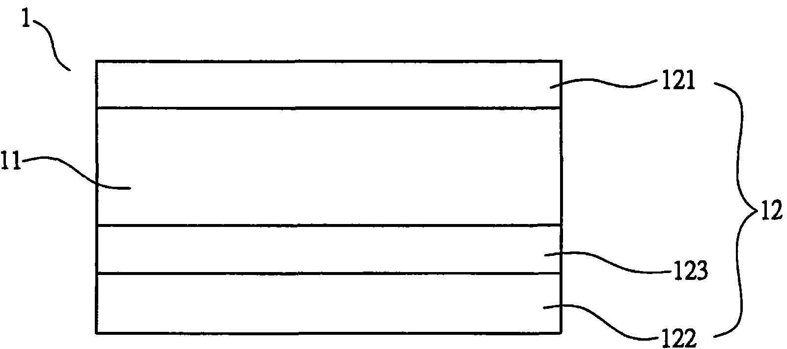
[0017] The present invention relates to a method for manufacturing a transparent conductive laminate. It mainly refers to the manufacturing method of the conductive laminate in the transparent conductive film. The transparent conductive film 2 includes at least one organic polymer substrate 21, and at least one laminate 22 is formed on the surface of the substrate 21, wherein the organic polymer substrate 21 Can include PC, PET... etc., at least one layer of the laminated body 22 can be a conductive layer 221 laminated mainly formed of indium tin oxide (ITO) material, the formation of the conductive layer 221 can be through Vacuum evaporation method, sputtering method, ion coating method, spray pyrolysis method, chemical plating method, electroplating method or their combination method to form, wherein preferred vacuum evaporation method, sputtering method, formed on the surface of substrate 21 After the conductive layer 221, it is irradiated with a light source with a specifi...


PUM

PropertyMeasurementUnit
wavelengthaaaaaaaaaa
porosityaaaaaaaaaa

Abstract

The invention relates to a method for manufacturing a transparent conductive lamination body and particularly provides a method for manufacturing a conductive lamination body in a transparent conductive film. In the method, a light source with a single-wavelength or specific broadband spectrum is adopted to irradiate a transparent conductive film to crystallize a conductive layer on the surface of the transparent conductive film and improve the performance of the optical and electrical characteristics of the transparent conductive film, and thus, the reliability of the transparent conductive film is realized and improved.

Description

technical field [0001] The present invention relates to a method for manufacturing a transparent conductive laminate, in particular to a method for forming a crystallized transparent conductive layer. Background technique [0002] It is well known that the transparent conductive film formed an indium tin oxide layer on the glass in the early days to become the so-called conductive glass, but the flexibility and processability of the glass material are poor, and the performance of impact resistance and light weight is also not good. Therefore, the transparent conductive film has been gradually replaced by various plastics mainly based on polyethylene terephthalate (PET). [0003] In the currently commercially available transparent conductive film structure, there is a transparent substrate made of plastic material, and there are multiple layers of laminates on the surface of the substrate; [0004] Such as figure 1 As shown, the transparent conductive film 1 has a substrate...

Claims


Application Information

Patent Timeline
Patent Type & Authority Applications(China)
IPC IPC(8): H01B13/00H01B5/14
Inventor 麦建进王湧锋尹瑞堂王剀弘
Owner GAMMA OPTICAL
Why Eureka
Try Eureka