Semiconductor laser device

A laser device and semiconductor technology, which is applied in the direction of semiconductor laser devices, semiconductor lasers, laser devices, etc., can solve the problem of not being able to sufficiently reduce the angle deviation of the polarization direction

Inactive Publication Date: 2012-07-04
KK TOSHIBA
View PDF1 Cites 0 Cited by
  • Summary
  • Abstract
  • Description
  • Claims
  • Application Information

AI Technical Summary

Problems solved by technology

[0007] However, even with this example, the angular deviation of the polarization direction cannot be sufficiently reduced

Method used


Image

  • Semiconductor laser device
  • Semiconductor laser device
  • Semiconductor laser device

Examples


Embodiment Construction

[0024] Hereinafter, embodiments of the present invention will be described with reference to the drawings.

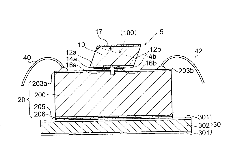
[0025] figure 1 is a schematic cross-sectional view of a semiconductor laser device according to an embodiment of the present invention.

[0026] The semiconductor laser device includes: a laser array 5 , a base 20 , alloy solder layers 16 , 207 and leads 30 .

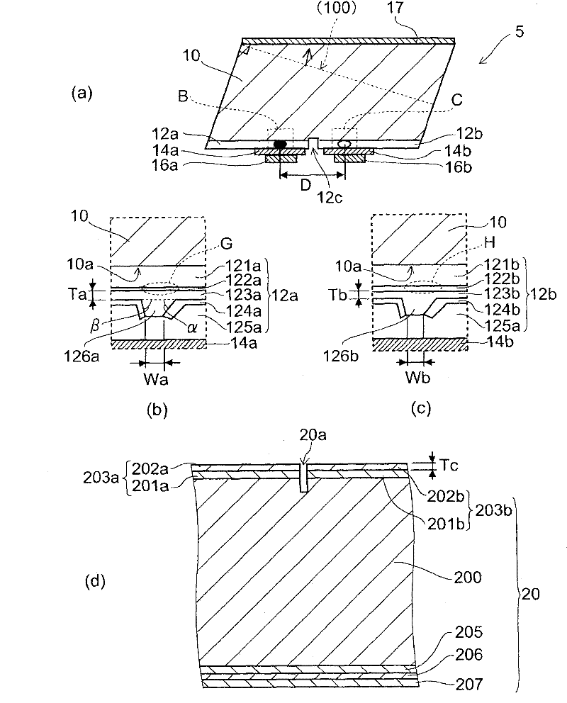
[0027] The laser array 5 has, on a semiconductor substrate 10 made of n-type GaAs or the like: a first stack 12a including a light-emitting layer, a second stack 12b including a light-emitting layer, and a first p-layer provided on the first stack 12a. The side electrode 14a, and the second p-side electrode 14b provided on the second laminated body 12b.

[0028] The base 20 has first and second conductive layers 203a, 203b on one face of the insulating material 200 . In addition, the base 20 has a backside conductive layer on the other side of the insulating material 200 . The first conductive layer 203a is ...


PUM


Abstract

The invention provides a semiconductor laser device, capable of reducing the angle deviation along the polarization direction, comprising a laser array composed of a first lamination body with a ridge type wave guide and sending the light of first wavelength, a second lamination body separated from a clamping groove and sending the light of second wavelength longer than the first wavelength, first, second electrodes containing gold films on the first, second lamination bodies; a bottom seat composed of an insulation body, a base metal film and first, second conductive layers of the gold film in the thickness of 0.05-03 Mum which are arranged on the insulation body in turn; a first alloy solder layer for joining the first electrode and the first conductive layer and having the thickness thicker than the gold film of the first conductive layer, wherein the inclination angle of the side surface of the ridge type wave guide near to the groove is smoother than the inclination angle of the side surface far away from the groove.

Description

technical field [0001] The present invention relates to semiconductor laser devices. Background technique [0002] Using a monolithic laser array in which semiconductor lasers with different wavelengths are integrated on one chip can simplify the structure of a DVD / CD compatible optical disc drive and facilitate miniaturization. [0003] The optical system of the optical disk drive device has optical elements such as a dichroic prism, a beam splitter, a collimator lens, a wave plate, an objective lens, and an erecting mirror. At this time, if the laser beams are brought close to each other at an interval of 100 to 150 μm, it is easy to satisfy the characteristics of the optical element at different wavelengths. [0004] However, in order to achieve further miniaturization, further simplification of the optical system is required. For this reason, it is important to further reduce fluctuations in the characteristic distribution of semiconductor lasers. [0005] When the ma...

Claims


Application Information

Patent Timeline
Patent Type & Authority Patents(China)
IPC IPC(8): H01S5/40H01S5/022H01S5/02H01S5/22
Inventor 玄永康一田中宏和弓削省三河本聪盐泽秀夫
Owner KK TOSHIBA
Why Eureka
Try Eureka