

Boost and buck integrated bridge-free power factor correction (PFC) circuit
A circuit, single-stage technology, used in electrical components, high-efficiency power electronic conversion, output power conversion devices, etc., can solve the problems of high conduction loss, low circuit efficiency, and high cost, reducing conduction loss and improving efficiency. , the effect of reducing costs
- Summary
- Abstract
- Description
- Claims
- Application Information
AI Technical Summary
Problems solved by technology
Method used
Image

Examples
Embodiment Construction
[0018] The present invention will be further described below in conjunction with drawings and embodiments.
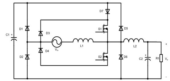
[0019] Refer to attached figure 1 , a specific implementation circuit diagram of a bridgeless single-stage PFC circuit integrated with a BOOST circuit and a BUCK circuit proposed by the present invention, including an AC input source Vin, a power MOSFET S1, a power MOSFET S2, a diode D1, a diode D2, and a diode D3, Diode D4, diode D5, diode D6, diode D7, energy storage capacitor C1, energy storage capacitor C2, inductance L1, inductance L2 and load equivalent resistance R1.
[0020] figure 1 The bridgeless single-stage PFC circuit adopts such a connection mode: one end of the AC input source Vin is connected to the anode of the diode D1, the anode of the diode D3, the cathode of the diode D2 and the cathode of the diode D4; the other end of the AC input source Vin Connect one end of the inductor L1; the other end of the inductor L1 is connected to the source of the p...
PUM
 Abstract
Description
Claims
Application Information