Light-emitting diode and manufacturing method thereof

A technology for light-emitting diodes and a manufacturing method, which is applied to semiconductor devices, electrical components, circuits, etc., can solve the problems of low luminous efficiency of light-emitting diodes, and achieve the effects of improving internal quantum efficiency and improving luminous efficiency.

Active Publication Date: 2011-04-20
BYD SEMICON CO LTD
View PDF0 Cites 12 Cited by
  • Summary
  • Abstract
  • Description
  • Claims
  • Application Information

AI Technical Summary

Problems solved by technology

[0004] In order to solve the technical problem of low luminous efficiency of light-emitting diodes, the present invent

Method used


Image

  • Light-emitting diode and manufacturing method thereof
  • Light-emitting diode and manufacturing method thereof
  • Light-emitting diode and manufacturing method thereof

Examples


Embodiment 1

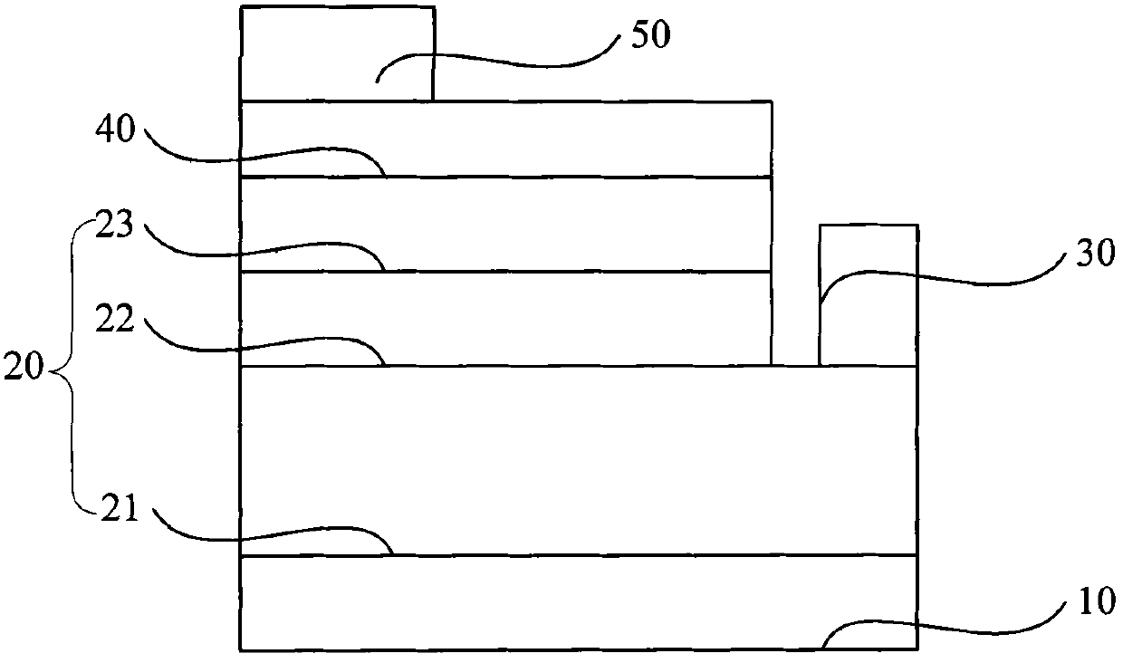
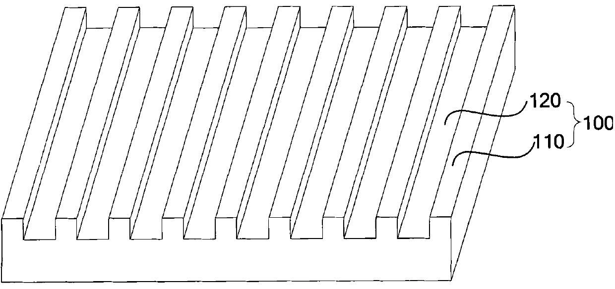
[0052] The light-emitting diode of Embodiment 1 provided by the present invention includes a substrate, a semiconductor layer, and a transparent conductive layer in sequence, and also includes a first electrode and a second electrode that can be electrically connected to the outside to provide electric energy to the light-emitting diode. The layer is electrically connected, and the second electrode is electrically connected to the transparent conductive layer; wherein, the upper surface of the substrate has several grooves and some protrusions; The semiconductor layer is located directly above the groove, the protruding semiconductor layer is located directly above the protrusion; the transparent conductive layer is located above the semiconductor layer, and is used to supply current to the semiconductor layer of the groove. The substrate is a patterned substrate. The semiconductor layer longitudinally includes a first semiconductor layer connected to the substrate, a light em...

Embodiment 2

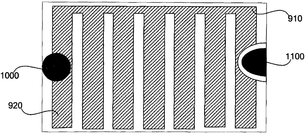
[0074] Please refer to Figure 5 The light-emitting diode according to the second embodiment of the present invention includes the patterned substrate 2100 described above, and above the patterned substrate 2100 are a nucleation layer 2200, a buffer layer 2300, an N-type semiconductor layer (first semiconductor layer) 2400, The light emitting layer 2500 , the second semiconductor barrier layer 2600 on the light emitting layer 2500 , the magnesium doped P type semiconductor layer 2700 , the heavily doped P type semiconductor layer 2800 with a rough structure 2810 , and the transparent conductive layer 2900 . The patterned substrate 2100 has grooves 2120 and protrusions 2110 . The light emitting diode of the embodiment of the present invention further includes an N-type electrode 21100 and a P-type electrode 21000 . There are two differences between the present embodiment and the first embodiment. One is that the structure of the transparent conductive layer of the light-emitti...

Embodiment 3

[0077] Please refer to Figure 6, the light-emitting diode of the third embodiment of the present invention is a light-emitting diode with a vertical structure, including: an N-type semiconductor layer (first semiconductor layer) 3400, a light-emitting layer 3500, a second semiconductor barrier layer 3600 located on the light-emitting layer 3500, magnesium A doped P-type semiconductor layer 3700 , a heavily doped P-type semiconductor layer 3800 with a rough structure 3810 , an insulating strip 31200 just covering the rough structure 2810 , and a bright conductive layer 3900 . The light emitting diode of the embodiment of the present invention further includes an N-type electrode 31100 and a P-type electrode 31000 . The N-type electrode 31100 is electrically connected to the N-type semiconductor layer 3400 and located below it, and the P-type electrode 31000 is electrically connected to the transparent conductive layer 2900 and located above it. The light emitting diode of thi...


PUM

PropertyMeasurementUnit
Thicknessaaaaaaaaaa
Thicknessaaaaaaaaaa
Widthaaaaaaaaaa

Abstract

The invention provides a light-emitting diode and a manufacturing method thereof. The light-emitting diode sequentially comprises a substrate, a semiconductor layer and a transparent conducting layer. The light-emitting diode also comprises a first electrode and a second electrode. The first electrode is electrically connected with the semiconductor layer, and the second electrode is electrically connected with the transparent conducting layer; the upper surface of the substrate is provided with a plurality of bulges, and grooves are formed among the bulges; the semiconductor layer comprises a groove semiconductor layer positioned over the grooves and a bulge semiconductor layer positioned over the bulges; and the transparent conducting layer is positioned above the semiconductor layer for providing current for the groove semiconductor layer. In the light-emitting diode, the current mainly passes through the groove semiconductor layer with less lattice defects and only a little current passes through the bulge semiconductor layer with more lattice defects so as to greatly reduce the occurrence probability of the nonradiative recombination and improve the lighting efficiency of the light-emitting diode.

Description

technical field [0001] The invention belongs to the field of semiconductor lighting, in particular to a light emitting diode and a manufacturing method thereof. Background technique [0002] Light-emitting diode (LED) is a junction electroluminescent semiconductor device that can convert electrical signals into optical signals. Gallium nitride (GaN)-based light-emitting diodes have been used as solid-state light sources for their high efficiency, long life, and energy saving. The advantages of environmental protection and small size are known as another revolution in the history of human lighting after Edison invented the electric light. It has become the focus of R&D and industry attention in the field of international semiconductors and lighting. ), aluminum gallium nitride (AlGaN) and aluminum indium gallium nitride (AlGaInN)-based III-V nitride materials have a continuously adjustable direct bandwidth of 0.7-6.2eV, covering the range from ultraviolet light to infrared li...

Claims


Application Information

Patent Timeline
IPC IPC(8): H01L33/20H01L33/22
CPCH01L33/20H01L33/44H01L33/42H01L33/38
Inventor 谢春林苏喜林胡红坡张旺
Owner BYD SEMICON CO LTD
Why Eureka
Try Eureka