Method for etching deep through silicon via (TSV)

A technology of deep silicon and etching depth, applied in chemical instruments and methods, processes for producing decorative surface effects, decorative arts, etc., can solve the problem of reducing silicon etching speed, difficult to achieve high-speed etching, reducing etching speed and other issues, to achieve the effects of good anisotropy, prolonged time, and high etching efficiency

Active Publication Date: 2014-02-12
ADVANCED MICRO FAB EQUIP INC CHINA
View PDF3 Cites 0 Cited by
  • Summary
  • Abstract
  • Description
  • Claims
  • Application Information

AI Technical Summary

Problems solved by technology

More protection to the sidewall will significantly reduce the etching rate of silicon, while the sidewall protection gas such as C 4 f 8 It will accumulate on the sidewall, and the longer the etching time, the more it will accumulate, and a thick accumulation layer will be formed at the opening of the etched silicon hole, which will affect the entry of reactive gases and further reduce the etching rate.
The single-step etching method needs to realize the etching in one etching process and ensure the protection of the sidewall during a long etching time, but with the increase of the etching depth, the accumulation of polymer and the decrease of the etching speed The reduction will affect the final performance. It is difficult to achieve high-speed etching and adequate protection of the sidewall with a single-step etching method

Method used


Image

  • Method for etching deep through silicon via (TSV)
  • Method for etching deep through silicon via (TSV)
  • Method for etching deep through silicon via (TSV)

Examples


no. 1 example

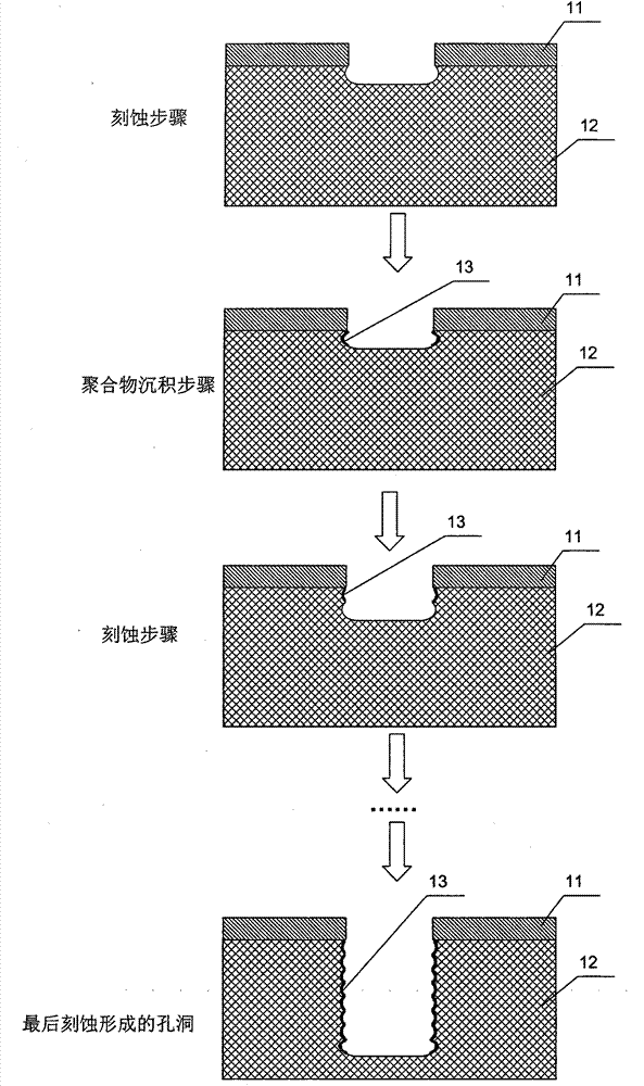
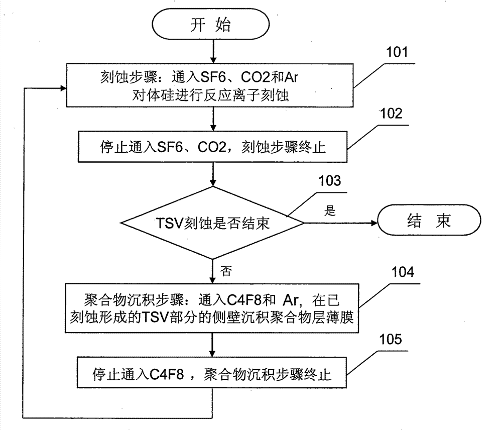
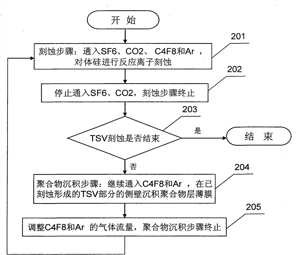
[0017] figure 2 Shown is a schematic flow chart of the TSV etching method according to the first embodiment of the present invention. In the TSV etching method, it is used to etch bulk silicon, and the shape parameters such as the depth, width, and aperture of the TSV through holes that are specifically required to be etched are not limited by the present invention, and can be determined according to different process conditions. In this example, 60 μm deep TSV vias are etched. The following specific steps are figure 2 The TSV etching method of the first embodiment shown is described in detail.

[0018] Step 101, etching step: injecting SF 6 , CO 2 and Ar, reactive ion etching of bulk silicon.

[0019] In this step, reactive ion etching is used to etch the bulk silicon, on which there are such figure 1 The mask layer shown in 11 is used to pattern the TSV. In this specific embodiment, the etching reaction chamber adopts the capacitively coupled plasma source technolog...


PUM


Abstract

The invention provides a method for etching a deep through silicon via (TSV), belonging to the technical field of semiconductor manufacturing. The etching method comprises a reaction ion etching step and a polymer deposition step which are alternately carried out, wherein gases adopted in the etching step comprise a first gas for chemical reaction plasma etching of silicon and a second gas which reacts with the silicon to form a silicide protection film. When used for etching the TSV, the etching method has the characteristics of high etching efficiency and good smoothness of the side wall of the TSV.

Description

technical field [0001] The invention belongs to the technical field of semiconductor manufacturing, and in particular relates to a reactive ion etching (Reactive Icon Etching, RIE) technology, in particular to a deep through silicon via (Through-Silicon-Via, TSV) etching method. Background technique [0002] In the field of semiconductor manufacturing technology, in fields such as MEMS (Micro-Electro-Mechanical Systems, micro-electro-mechanical systems) and 3D packaging technology, it is usually necessary to etch deep via holes in materials such as silicon. For example, in bulk silicon etching technology, deep through-silicon-vias (Through-Silicon-Via, TSV) have a depth of hundreds of microns, and their aspect ratio is even much greater than 10. Reactive ion etching is usually used to etch the bulk silicon. silicon formed. [0003] figure 1 Shown is a schematic diagram of an etching method for deep TSVs in the prior art. In the prior art, the reactive ion etching of TSVs ...

Claims


Application Information

Patent Timeline
Patent Type & Authority Patents(China)
IPC IPC(8): C23F1/02C23F1/12C30B33/12B81C1/00H01L21/3065H01L21/308
Inventor 崔在雄凯文·皮尔斯吴万俊严利均雷本亮
Owner ADVANCED MICRO FAB EQUIP INC CHINA
Why Eureka
Try Eureka