Substrate with self-stripping function and method for stripping epitaxial layer

An epitaxial layer, self-stripping technology, applied in the direction of electrical components, electrical solid devices, circuits, etc., can solve the problem of low cost, achieve the effect of short process cycle, low cost, and not easy to surface cracks

Inactive Publication Date: 2011-04-27
SUZHOU NANOWIN SCI & TECH
View PDF0 Cites 6 Cited by
  • Summary
  • Abstract
  • Description
  • Claims
  • Application Information

AI Technical Summary

Problems solved by technology

In the prior art, it is still impossible to find a lift-off process that can completely overcome the defects of the...

Method used


Image

  • Substrate with self-stripping function and method for stripping epitaxial layer
  • Substrate with self-stripping function and method for stripping epitaxial layer
  • Substrate with self-stripping function and method for stripping epitaxial layer

Examples


no. 1 Embodiment approach

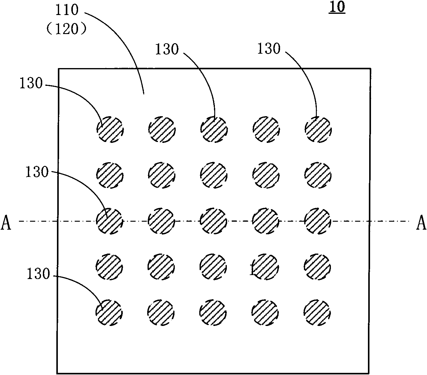
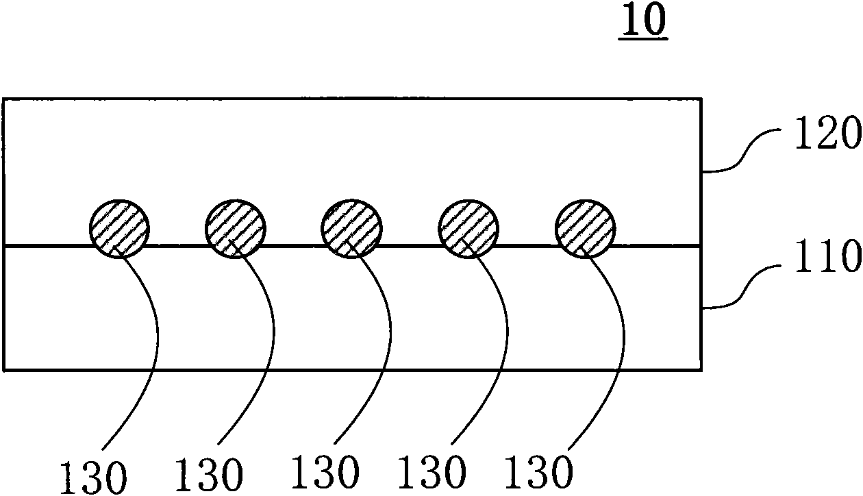
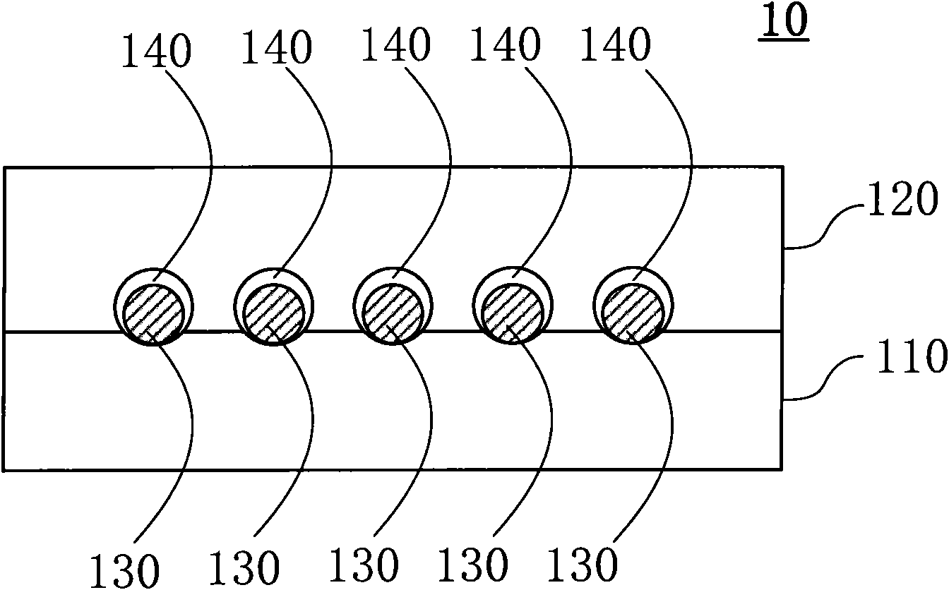
[0053] attached Figure 5 Shown is a schematic diagram of the implementation steps of this specific embodiment, including; step S20, providing a support substrate; step S21, forming a plurality of thermoelastic bodies on the surface of the support substrate, and the plurality of thermoelastomers are formed on the surface of the support substrate Two-dimensional distribution; step S22, further forming an epitaxial layer on the surface of the support substrate formed with a plurality of thermoelastomers, and the epitaxial layer completely covers the surface of the thermoelastomer and the support substrate; step S23, raising the temperature of the system, A cavity is formed at the position of the thermoelastomer; step S24, applying a shear force between the epitaxial layer and the supporting substrate to separate them; step S25, removing the thermoelastomer attached to the surface of the epitaxial layer.

[0054] In this specific embodiment, the thermoelastic body 130 is a plural...


PUM

PropertyMeasurementUnit
Diameteraaaaaaaaaa

Abstract

The invention discloses a substrate with a self-stripping function, comprising a supporting substrate and an epitaxial layer arranged on the surface of the supporting substrate, wherein the supporting substrate has a first thermal expansion coefficient; the epitaxial layer has a second thermal expansion coefficient; the substrate further comprises a thermoplastic elastomer arranged at the interface of the supporting substrate and the epitaxial layer and has the third thermal expansion coefficient; and the function for stripping the epitaxial layer can be achieved by changing the temperature of the thermoplastic elastomer in the stripping layer. As an optional technical scheme, the third thermal expansion coefficient is smaller than the smaller one of the first thermal expansion coefficient and the second thermal expansion coefficient or greater than the greater one of first thermal expansion coefficient and the second thermal expansion coefficient. The technical scheme of the invention has the advantages of realizing the stripping process with low cost, high efficiency and no damage to the epitaxial layer.

Description

【Technical field】 [0001] The invention relates to the field of semiconductor materials, in particular to a substrate with a peeling layer and a method for automatically peeling off an epitaxial layer. 【Background technique】 [0002] The preparation of semiconductor materials, especially compound semiconductor materials, usually forms a thin film material with a certain thickness on the surface of a specific substrate by chemical deposition or other means. For example, compound semiconductor materials such as GaN, ZnO, or InP are epitaxially grown on the surface of sapphire or silicon substrates, and materials such as SiGe, SiC, or stressed silicon are epitaxially grown on the surface of single crystal silicon substrates. After a certain thickness of epitaxial material is obtained, the substrate and the epitaxial layer are sometimes separated from each other due to the needs of device structure and other aspects, or it is called the stripping process of the epitaxial layer. ...

Claims


Application Information

Patent Timeline
IPC IPC(8): H01L23/00H01L21/02H01L21/20H01L21/301
Inventor 王建峰任国强刘建奇徐科
Owner SUZHOU NANOWIN SCI & TECH
Why Eureka
Try Eureka