High-voltage double-diffused metal-oxide-semiconductor (DMOS) device

A device and high-voltage technology, which is applied in the field of DMOS devices, can solve the problems of reducing device performance and increasing on-resistance, and achieve the effects of reducing electric field, increasing breakdown voltage, and reducing the possibility of breakdown

Inactive Publication Date: 2011-05-04
SHANGHAI HUA HONG NEC ELECTRONICS
View PDF0 Cites 2 Cited by
  • Summary
  • Abstract
  • Description
  • Claims
  • Application Information

AI Technical Summary

Problems solved by technology

[0003] In traditional devices, because the electric field is easy to concentrate on the surface of the drift region of the device, the breakdown voltage of the device is reduced. In order to make the breakdown voltage of the device reach a higher value, a traditional method is to reduce the doping concentration of the drift region or increase The size of the drift region increases the on-resistance of the drift region, but this reduces the performance of the device

Method used


Image

  • High-voltage double-diffused metal-oxide-semiconductor (DMOS) device
  • High-voltage double-diffused metal-oxide-semiconductor (DMOS) device
  • High-voltage double-diffused metal-oxide-semiconductor (DMOS) device

Examples


Embodiment Construction

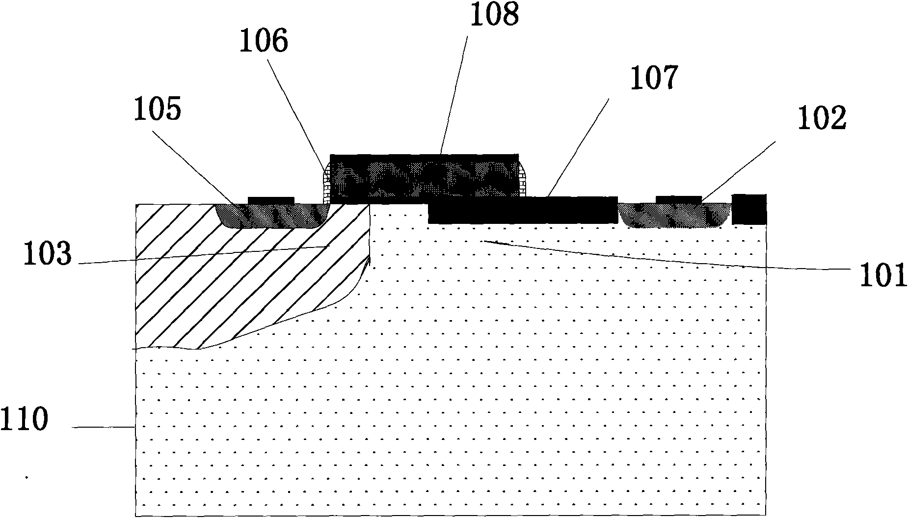
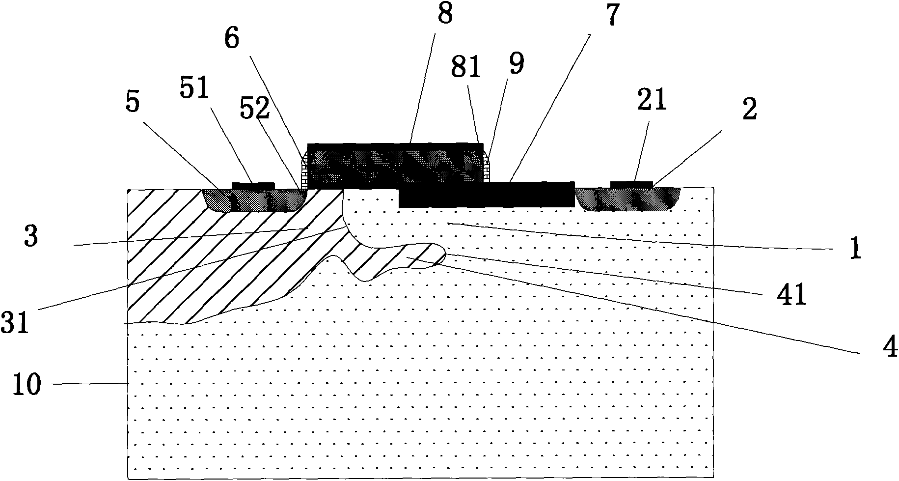
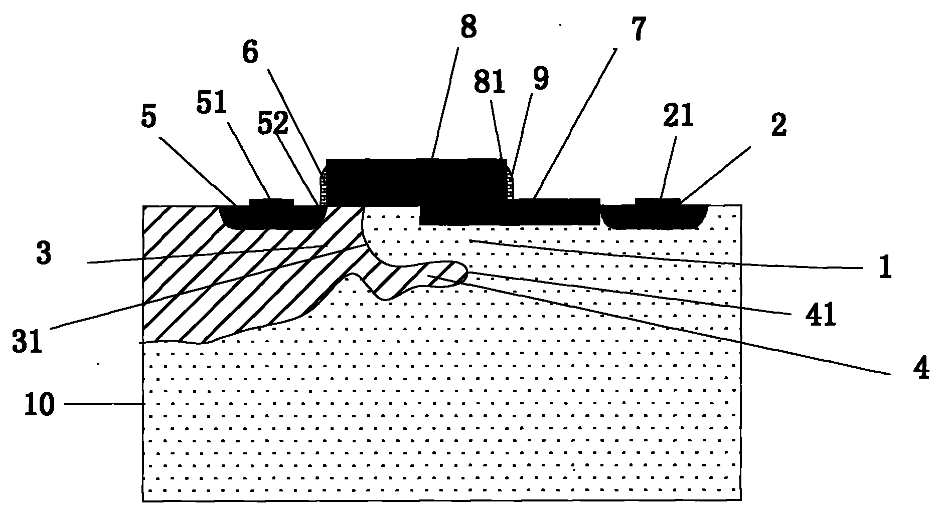
[0011] like figure 2 As shown, the embodiment of the present invention mainly includes: a drift region 1, a drain region 2, a channel region 3, a source region 5, a gate oxide layer 6, a field oxide layer 7, a gate 8 and a buried Layer 4.

[0012] On a substrate with the first conductivity type (the substrate is in figure 2 (not shown in ) to form a well region 10 with the second conductivity type, and the drift region 4 is a part of the well region 10 between the channel region 3 and the drain region 2 . The drain region 2 , formed in the well region 10 and connected to one end of the drift region 1 , has a second conductivity type, and a drain terminal 21 is formed in the drain region 2 . The channel region 3, formed in the well region 10 and connected to the other end of the drift region 1, has the first conductivity type. The source region 5 is formed in the channel region 3 and has the second conductivity type, and a source terminal 51 is formed in the source region ...


PUM


Abstract

The invention discloses a high-voltage double-diffused metal-oxide-semiconductor (DMOS) device, comprising a drift region, a drain region, a channel region, a source region, a gate oxidation layer, a gate and a buried layer, wherein the drift region is positioned between the channel region and the gate region; the source region is formed on the channel region; and the buried layer is buried in the drift region and connected with the channel region. The buried layer and the channel region is respectively provided with a first conducting type, and the source region, the drain region and the drift region are respectively provided with a second conducting type. The buried layer can guide high potential of the drift region introduced by the drain region to a deep part of the drift region, so that the electric field of the drift region is two-dimensionally uniformly distributed, the accumulation of the electric field on the surface of the drift region is reduced, and therefore, the breakdown probability occurring on the surface of the drift region is reduced, and the breakdown voltage is increased. On the basis of increasing the breakdown voltage, by increasing the doping concentration of the drift region or reducing the size of the device, the on resistance of the DMOS can be reduced and the characteristics of the device can be improved.

Description

technical field [0001] The invention relates to a DMOS device, in particular to a high-voltage DMOS device with high breakdown voltage and low conduction resistance and its manufacturing process. Background technique [0002] like figure 1 Shown is a schematic cross-sectional view of a traditional high-voltage DMOS device. A conventional high voltage device includes a well region 110 in which a source region 105 , a drain region 102 , a channel region 103 and a drift region 101 are formed. A gate oxide layer 106 is formed on the channel region, and a field oxide layer 107 is formed on the drift region and in the isolation region between devices. The gate 108 covers the gate oxide layer 106 and covers a part of the field oxide layer 107 . When a traditional high-voltage DMOS device is working, a high voltage is applied between the source and the drain, and the PN junction formed between the drift region and the channel is under the action of a high reverse bias at the drai...

Claims


Application Information

Patent Timeline
Patent Type & Authority Applications(China)
IPC IPC(8): H01L29/78H01L29/06H01L21/336H01L21/265
Inventor 钱文生
Owner SHANGHAI HUA HONG NEC ELECTRONICS
Why Eureka
Try Eureka