Electrostatic multipole lens

A technology of electronic lens and electron column, which is applied in the direction of circuits, discharge tubes, electrical components, etc., can solve problems such as difficulty in manufacturing, control and alignment, and influence on the resolution of electron columns, and achieve small electron beam spots and improve resolution , the effect of reducing the number of

Inactive Publication Date: 2011-05-04
CEBT
View PDF3 Cites 6 Cited by
  • Summary
  • Abstract
  • Description
  • Claims
  • Application Information

AI Technical Summary

Problems solved by technology

Electron beam enlargement due to astigmatism and beam distortion can negatively affect the resolution of the electron column
[0012] In addition, traditional octopole lenses and other multipole lenses are difficult to manufacture, control, and align due to the multiple electrodes distributed on a single lens layer

Method used


Image

  • Electrostatic multipole lens
  • Electrostatic multipole lens
  • Electrostatic multipole lens

Examples


Embodiment Construction

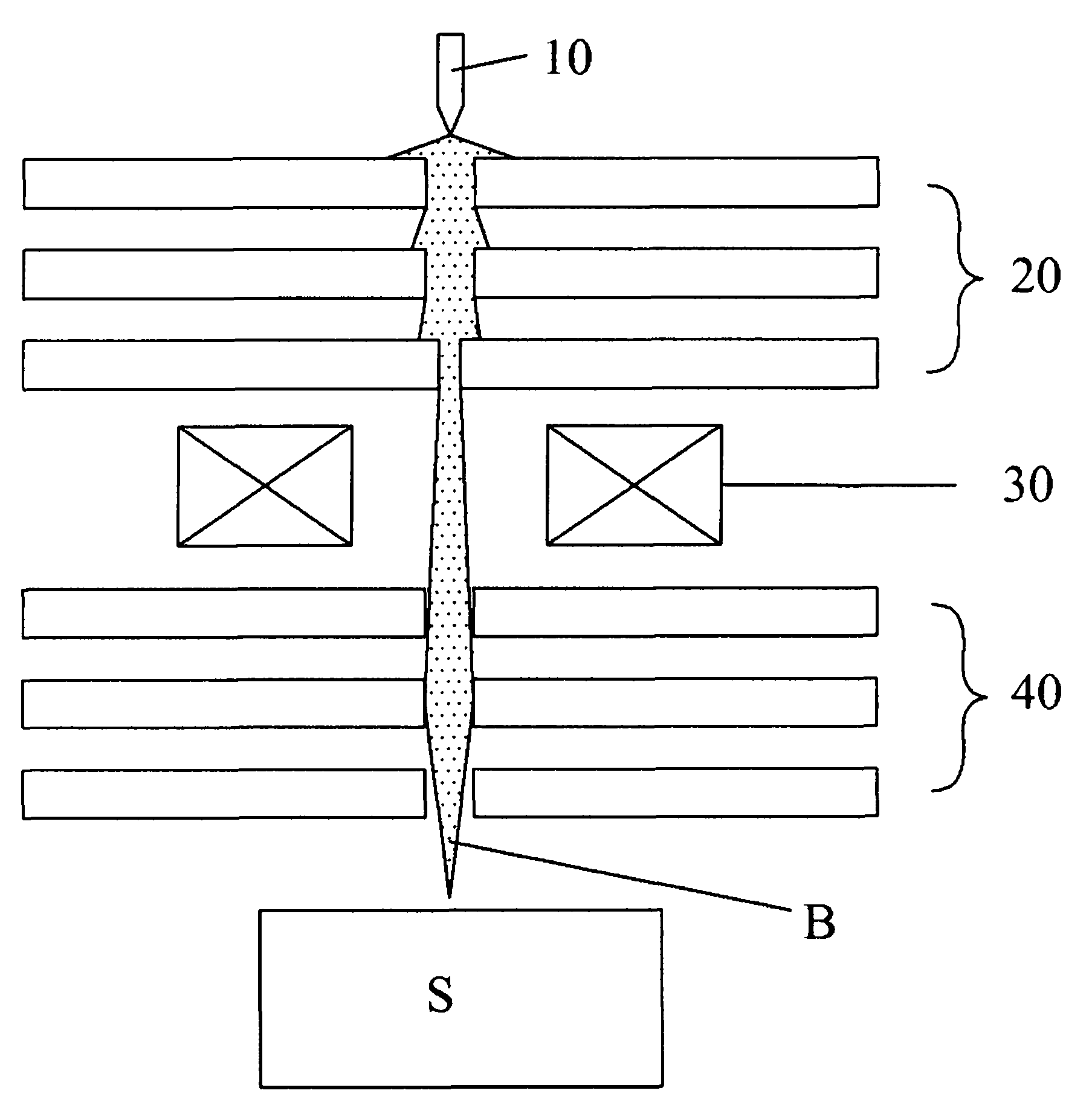
[0038] The present invention is provided for forming a low aberration, high resolution electron beam spot by using a multipole lens within an electron column.

[0039] The invention provides an electrostatic multipole lens, which can not only correct the astigmatism, but also correct the deformation of the beam spot of the whole deflection field, so as to improve the performance of the electron column.

[0040] The structure of the electrostatic multipole lens of the present invention is simple, and by using the multipole lens in the focusing lens, the beam spot of the electron beam generated by various types of distortion generated around the sample by the electron beam scanned by the electron column is reduced deflection defocus.

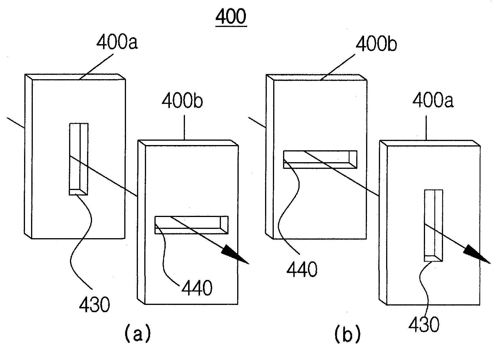
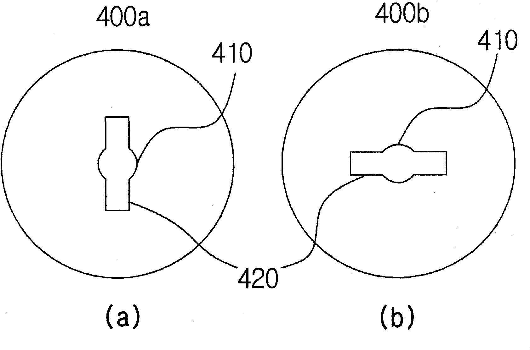
[0041] figure 2 One example of a multipole lens with a simple structure and orthogonal apertures is schematically shown.

[0042] exist figure 2 , each quadrupole lens 400 (i.e., a multipole lens for electro-optical design) is configured to i...


PUM


Abstract

The present invention relates to an electron lens for use in an microcolumn, and more particularly to a multipole electron lens wherein the electron lens includes two or more electrode layers, each of the electrode layers has a slit extending from a central axis through which an electron beam passes, and the two electrode layers are aligned on an electron optical axis such that the slits are staggered with each other. Further, the present invention relates to a microcolumn using the multipole lens. The multipole lens according to the present invention can be manufactured and controlled in a simple fashion, reduces blurring of the focus of the microcolumn, and increases an active deflective area.

Description

technical field [0001] The present invention relates to electron lenses, and more particularly to a multipole electron lens for minimizing the electron-optical viewpoint by an electron lens that controls an electron beam in an electron column such as a microcolumn. Electron beam distortion caused by aberrations in Background technique [0002] The electron column includes an electron emission source and an electron lens, creates and scans an electron beam, and is used in an electron microscope, semiconductor lithography, or inspection equipment using an electron beam, such as an apparatus for inspecting a via hole / contact hole of a semiconductor device, for Devices for inspecting and analyzing sample surfaces, or devices for inspecting thin-film transistors (TFTs) of TFT-LCD devices. [0003] Representative examples of such electron columns are microcolumns. Micropillars based on electron emission sources and electron-optical parts with fine structures were first introduce...

Claims


Application Information

Patent Timeline
Patent Type & Authority Applications(China)
IPC IPC(8): H01J37/147
CPCH01J37/12H01J37/28H01J2237/1205H01J2237/121H01J2237/153H01J2237/1532H01J2237/1534H01J2237/1536
Inventor 金浩燮吴泰植
Owner CEBT
Why Eureka
Try Eureka