

Improved development process for light beam homogenization device
A beam and laser beam technology, applied in optics, optical components, instruments, etc., can solve problems such as restricted processing capability, difficulty in ensuring lens curvature and surface accuracy, and difficulty in obtaining uniformity of light spots.
- Summary
- Abstract
- Description
- Claims
- Application Information
AI Technical Summary
Problems solved by technology
Method used
Image

Examples
Embodiment Construction
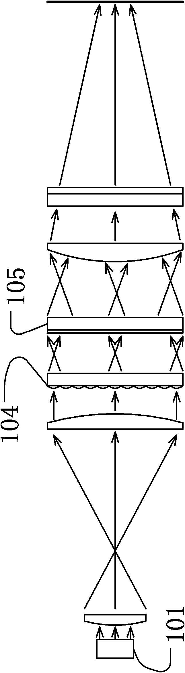
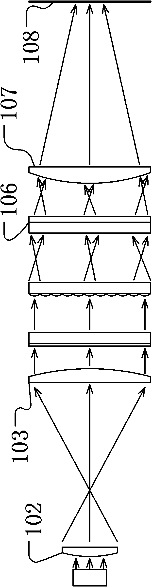
[0025] The purpose of the present invention is to propose an improved optical device for laser beam homogenization, which can be used in laser annealing equipment or other occasions where the beam needs to be homogenized. Adding the pre-homogenization link in the system, as well as the organic combination of different types of homogenization principle schemes, not only greatly reduces the processing difficulty of each optical element in the homogenization system, but also can obtain better homogenization effect.
[0026] The pre-homogenization link device proposed by the present invention is located before the common optical homogenization system, and it performs preliminary homogenization on the light beam and then enters the subsequent optical system to obtain further homogenization. In this way, through multi-level homogenization, a light spot with extremely high uniformity is finally obtained, and at the same time, the requirement for processing capacity is reduced.
[002...
PUM
 Abstract
Description
Claims
Application Information