Thin film transistor and manufacturing method thereof

A technology of thin-film transistors and manufacturing methods, which is applied in the direction of transistors, semiconductor/solid-state device manufacturing, semiconductor devices, etc., can solve problems such as the influence of component characteristics, and achieve the effect of optimal component characteristics

Active Publication Date: 2011-05-11
AU OPTRONICS CORP
View PDF4 Cites 10 Cited by
  • Summary
  • Abstract
  • Description
  • Claims
  • Application Information

AI Technical Summary

Problems solved by technology

However, it has been proved by experiments that the structural characteristics of the polysilicon thin film transistor formed by the above method will be affected by the etching process of the channel layer, and the device characteristics will be obviously affected by the structure of the channel layer

Method used


Image

  • Thin film transistor and manufacturing method thereof
  • Thin film transistor and manufacturing method thereof
  • Thin film transistor and manufacturing method thereof

Examples


no. 1 example

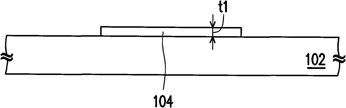
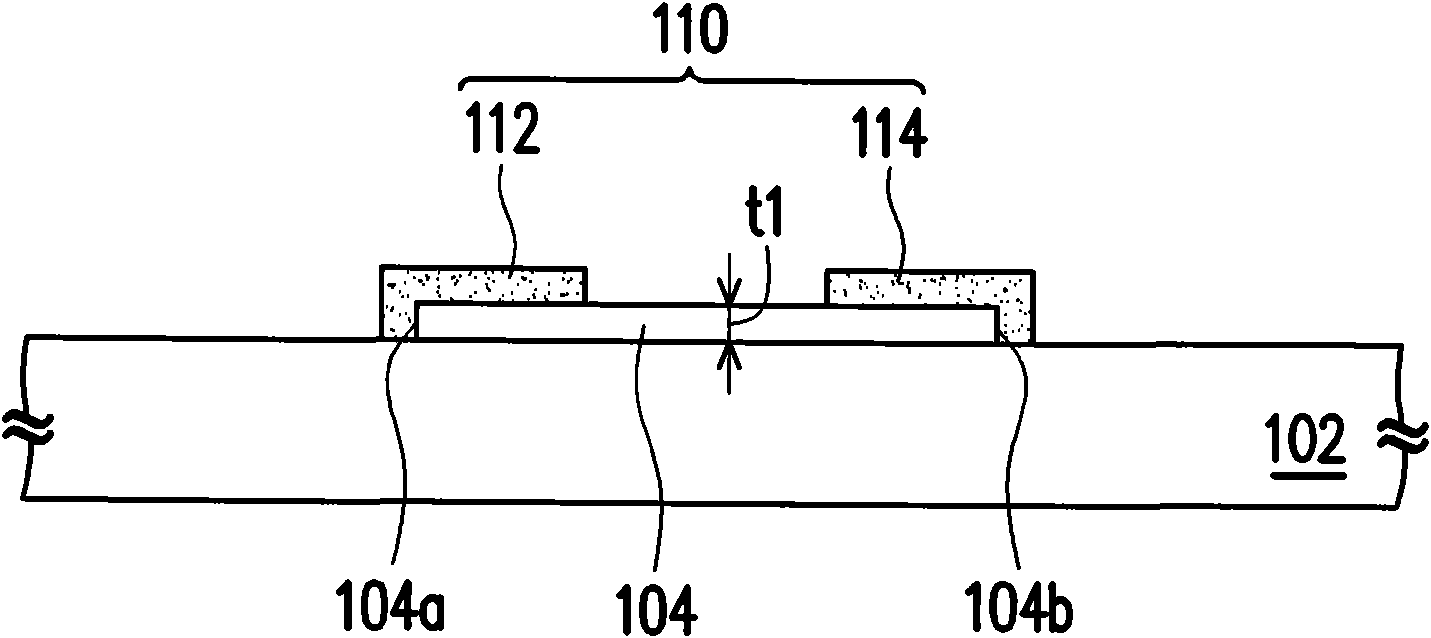
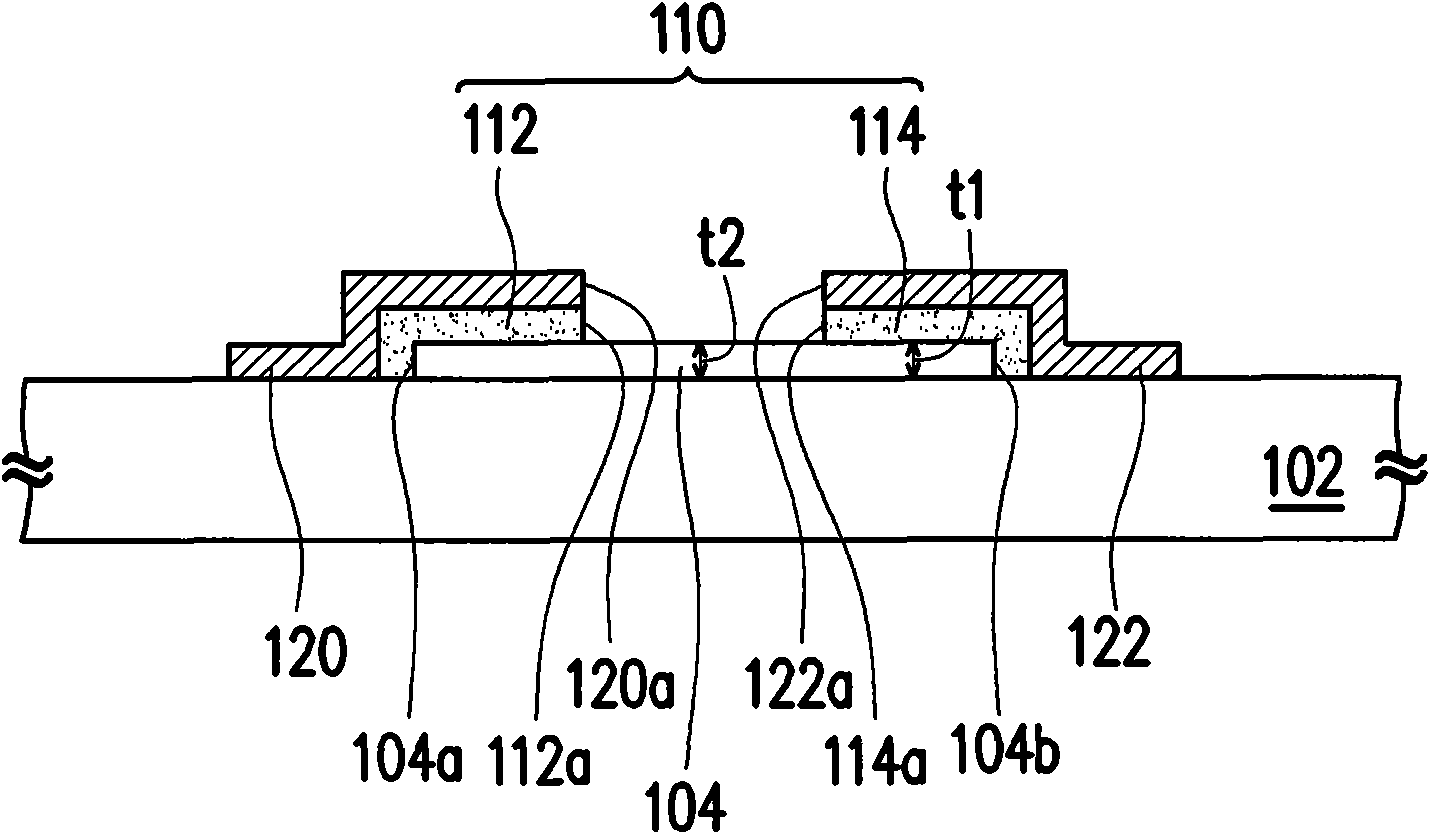
[0049] Figure 1A to Figure 1D It is a schematic cross-sectional flow diagram of a manufacturing method of a thin film transistor according to the first embodiment of the present invention. Please refer to Figure 1A , firstly, a semiconductor layer 104 is formed on a substrate 102, and the semiconductor layer 104 has a first thickness t1. In this embodiment, the substrate 102 may be a glass substrate, a quartz substrate or other material substrates, which is not limited in the present invention. The semiconductor layer 104 is, for example, a polysilicon layer, and its formation method is, for example, a deposition method or a crystallization method. In this embodiment, for example, an amorphous silicon layer (not shown) is formed on the substrate 102 first, and then the amorphous silicon is crystallized by solid phase crystallization (SPC), excimer laser (ELA) layer into a polysilicon layer. Wherein, the first thickness t1 is, for example, between 200 angstroms to 800 angs...

no. 2 example

[0058] Figure 2A to Figure 2D It is a schematic cross-sectional flow diagram of a manufacturing method of a thin film transistor according to the second embodiment of the present invention. Please refer to Figure 2A , firstly, a semiconductor layer 104 is formed on a substrate 102, and the semiconductor layer 104 has a first thickness t1. In this embodiment, the substrate 102 may be a glass substrate, a quartz substrate or other material substrates. The semiconductor layer 104 is, for example, a polysilicon layer, and its formation method is, for example, a deposition method or a crystallization method. In this embodiment, for example, an amorphous silicon layer (not shown) is formed on the substrate 102 first, and then the amorphous silicon is crystallized by solid phase crystallization (SPC), excimer laser (ELA) layer into a polysilicon layer. Wherein, the first thickness t1 is, for example, between 300 angstroms and 2000 angstroms.

[0059] Please refer to Figure 2...


PUM


Abstract

The invention discloses a thin film transistor and a manufacturing method thereof. The thin film transistor comprises a substrate, a semiconductor layer, a patterning doped semiconductor layer, a source electrode, a drain electrode, a grid isolating layer and a grid electrode, wherein the semiconductor layer is arranged on the substrate; the patterning doped semiconductor layer is arranged above two opposite sides of the semiconductor layer; the source electrode and the drain electrode are arranged on the patterning doped semiconductor layer and above two opposite sides of the semiconductor layer; a part of the semiconductor layer covered by the source electrode and the drain electrode has a first thickness, a part of the semiconductor layer, which is positioned between the source electrode and the drain electrode and not covered by the source electrode and the drain electrode, has a second thickness, and the second thickness is between 200 angstroms and 800 angstroms; the grid isolating layer is arranged on the source electrode, the drain electrode and a part of semiconductor layer; and the grid is arranged on the grid isolating layer. The thin film transistor provided by the invention has better element characteristics.

Description

technical field [0001] The present invention relates to a semiconductor element and its manufacturing method, and in particular to a thin film transistor and its manufacturing method. Background technique [0002] In recent years, with the increasing maturity of optoelectronic technology and semiconductor manufacturing technology, flat-panel displays have flourished. Among them, liquid crystal displays have gradually replaced traditional cathodes based on their advantages of low-voltage operation, no radiation scattering, light weight, and small size. Ray tube displays have become the mainstream of display products in recent years. In general, liquid crystal displays can be classified into two types: amorphous silicon thin film transistor liquid crystal displays and low temperature poly-silicon thin film transistor liquid crystal displays. [0003] Because low-temperature polysilicon thin film transistors have higher carrier mobility and better device stability, they are wi...

Claims


Application Information

Patent Timeline
Patent Type & Authority Applications(China)
IPC IPC(8): H01L29/786H01L29/06H01L21/336
Inventor 陈昶亘
Owner AU OPTRONICS CORP
Why Eureka
Try Eureka