Method for manufacturing T-shaped grid of GaN microwave device

A microwave device and manufacturing method technology, which is applied in semiconductor/solid-state device manufacturing, semiconductor devices, electrical components, etc., can solve the problems of reducing the reliability of GaN-based power devices, demanding process conditions, and poor process repeatability and stability. , to achieve the effect of improving gate characteristics and noise characteristics, optimizing gate morphology, and high controllability

Active Publication Date: 2011-05-18
THE 13TH RES INST OF CHINA ELECTRONICS TECH GRP CORP
View PDF8 Cites 4 Cited by
  • Summary
  • Abstract
  • Description
  • Claims
  • Application Information

AI Technical Summary

Problems solved by technology

The biggest disadvantage of this method is that it has strict requirements on the process conditions, the shape of the gate is not easy to control, and the repeatability and stability of the process are poor; moreover, there are often voids between the gate foot and the dielectric film in the fabricated T-shaped gate structure. Disadvantages that the gate metal cannot be fully filled, such as the Chinese patents with application numbers 00105221.7 and 02124062.0; the existence of air conditioners greatly reduces the reliability of GaN-based power devices

Method used


Image

  • Method for manufacturing T-shaped grid of GaN microwave device
  • Method for manufacturing T-shaped grid of GaN microwave device
  • Method for manufacturing T-shaped grid of GaN microwave device

Examples


Embodiment Construction

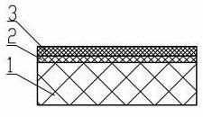
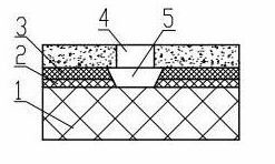
[0018] see Figure 1-Figure 7 , the steps of preparing the T-shaped grid of the present invention are as follows:

[0019] ①Grow a high-temperature dielectric layer 2 on the GaN substrate 1, and the composition of the high-temperature dielectric layer 2 is Si 3 N 4 .

[0020] First, the surface of the GaN substrate 1 is cleaned, and the cleaning steps are: soak in trichloroethane for 5-10 minutes; soak in acetone for 5-10 minutes; soak in isopropanol for 5-10 minutes; finally rinse with deionized water for 5-10 minutes. minute.

[0021] Then use MOVCD (Metal-organic Chemical Vapor DePosition, metal organic compound chemical vapor deposition method) growth process to make Si 3 N 4 , the growth temperature is 1000°C-1200°C, Si 3 N 4 The thickness is 100 angstroms ± 20 angstroms.

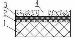
[0022] ②Grow a low-temperature dielectric layer 3 on the upper surface of the above-mentioned high-temperature dielectric layer 2, and the composition of the low-temperature dielectric layer 3 i...


PUM

PropertyMeasurementUnit
thicknessaaaaaaaaaa
thicknessaaaaaaaaaa
sizeaaaaaaaaaa

Abstract

The invention discloses a method for manufacturing a T-shaped grid of a GaN microwave device. The method comprises the following steps: (1) growing a high temperature dielectric layer on a GaN substrate, wherein the ingredient of the high temperature dielectric layer is Si3N4; (2) growing a low temperature dielectric layer on the upper surface of the high temperature dielectric layer, wherein the ingredient of the low temperature dielectric layer is SiOxNy; (3) photoetching a grid groove photoetched pattern in a required size on the low temperature dielectric layer, etching a grid groove on the low temperature dielectric layer and the high temperature dielectric layer through dry etching and removing the residual photoresist; (4) photoetching a grid cover photoetched pattern aligned with the grid groove on the low temperature dielectric layer; and (5) manufacturing a Schottky electrode on the GaN substrate in the grid cover pattern. By adopting the method, the grid length is easier to control and the reliability of the GaN microwave device is improved.

Description

technical field [0001] The invention relates to a method for designing and manufacturing a structure of a semiconductor device, in particular to a method for manufacturing a T-shaped gate of a GaN microwave device. Background technique [0002] GaN materials have excellent characteristics such as wide bandgap, high critical breakdown electric field, high thermal conductivity, and high carrier saturation drift velocity, which determine the advantages of GaN-based power devices based on them in the microwave and millimeter wave fields. . [0003] The continuous improvement of frequency characteristics makes the gate fabrication process of GaN-based power devices mainly adopt non-contact lithography technology (such as electron beam direct writing technology, stepping projection lithography technology, etc.) for gate fabrication. The commonly used methods are: in GaN Three layers of photoresist are coated on the substrate, and a photolithography is performed to obtain a gate p...

Claims


Application Information

Patent Timeline
Patent Type & Authority Applications(China)
IPC IPC(8): H01L21/28H01L21/338H01L29/78
Inventor 王勇李亮秘瑕彭志农周瑞蔡树军
Owner THE 13TH RES INST OF CHINA ELECTRONICS TECH GRP CORP
Why Eureka
Try Eureka