
Method for forming self-aligned contact hole by taking undoped silicon oxide as polycrystalline silicon cap layer

A self-aligned contact hole and polysilicon layer technology, which is applied in semiconductor/solid-state device manufacturing, electrical components, circuits, etc., can solve problems that are not conducive to the realization of double gate technology

Active Publication Date: 2011-05-18
SHANGHAI HUAHONG GRACE SEMICON MFG CORP
View PDF3 Cites 10 Cited by
  • Summary
  • Abstract
  • Description
  • Claims
  • Application Information

AI Technical Summary

Problems solved by technology

However, since silicon nitride has a very strong impurity blocking ability, this process method is not conducive to the realization of a self-aligned double gate process (Self-Align Dual Poly Process: that is, self-aligned polysilicon doping is achieved through source-drain implantation. )

Method used


Image

  • Method for forming self-aligned contact hole by taking undoped silicon oxide as polycrystalline silicon cap layer
  • Method for forming self-aligned contact hole by taking undoped silicon oxide as polycrystalline silicon cap layer
  • Method for forming self-aligned contact hole by taking undoped silicon oxide as polycrystalline silicon cap layer

Examples


Embodiment Construction

[0023] The present invention will be described in further detail below in conjunction with the accompanying drawings and embodiments.

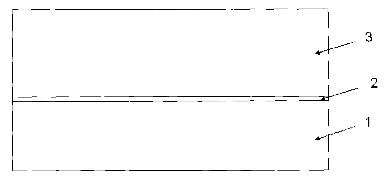
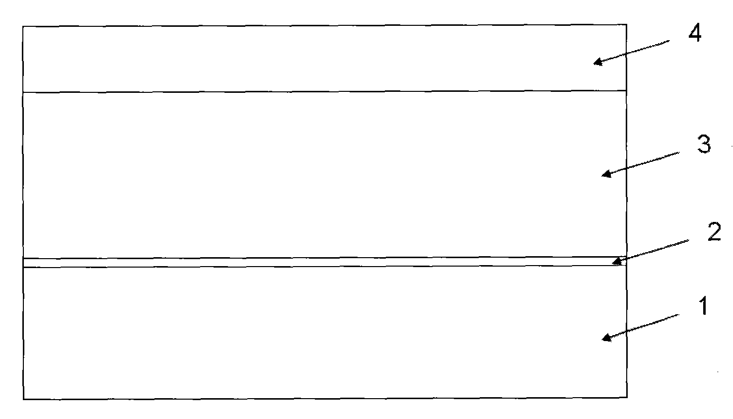
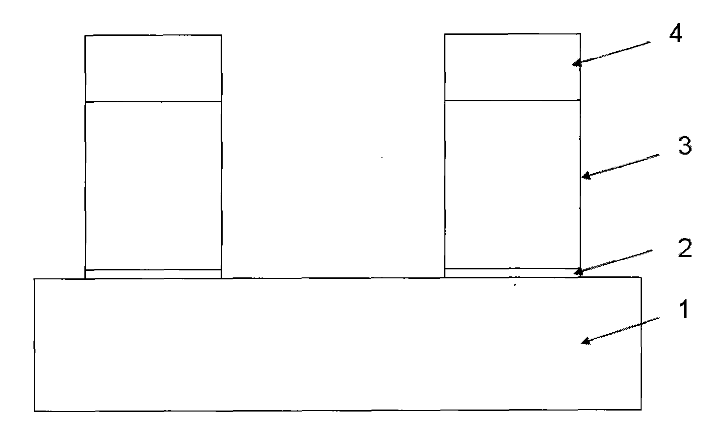
[0024] The invention provides a process method for making a self-aligned contact hole by using non-doped silicon oxide as a polysilicon cap layer. The PMD layer is made of phosphosilicate glass (PSG). In the contact hole etching, the self-alignment process is realized by controlling the high etching selectivity of the phosphosilicate glass and non-doped silicon oxide. On the other hand, due to the weak blocking ability of silicon oxide impurities, self-aligned polysilicon doping can be realized at the same time of source-drain implantation, thereby realizing a self-aligned double-gate process.

[0025] Main technological process of the present invention comprises the steps:

[0026] The first step, polysilicon deposition. Such as figure 1 As shown, according to the conventional process, the gate oxide layer 2 is first deposited on the silic...


PUM

PropertyMeasurementUnit
thicknessaaaaaaaaaa
thicknessaaaaaaaaaa
thicknessaaaaaaaaaa

Abstract

The invention discloses a method for forming a self-aligned contact hole by taking undoped silicon oxide as a polycrystalline silicon cap layer. The method comprises the following steps of: 1, depositing a grid oxide layer on a silicon substrate and depositing a polycrystalline silicon layer on the grid oxide layer; 2, depositing an undoped silicon oxide cap layer on the polycrystalline silicon layer; 3, photoetching and etching polycrystalline silicon so as to form a polycrystalline silicon electrode; 4, injecting a laser detector diode (LDD); 5, manufacturing a side wall of the polycrystalline silicon; 6, performing source drain injection and thermally annealing quickly; 7, preparing a phosphorosilicate glass physical medium dependent (PMD) layer on a full silicon chip; and 8, etching the self-aligned contact hole. By the method, self-aligned polycrystalline silicon doping can be realized during source drain injection, so that the realization of a self-aligning double grid process is facilitated.

Description

technical field [0001] The invention belongs to the field of semiconductor integrated circuit manufacturing, in particular to a method for making self-aligned contact holes by using non-doped silicon oxide as a polysilicon cap layer. Background technique [0002] In a conventional CMOS (Complementary Metal Oxide Semiconductor) process, silicon nitride is usually used as a cap layer on polysilicon for self-aligned contact holes. In the etching process of the contact hole, the self-alignment process is realized by controlling the etching selectivity ratio of the PMD layer (pre-metal dielectric layer) and silicon nitride by etching. However, since silicon nitride has a very strong impurity blocking ability, this process method is not conducive to the realization of a self-aligned double gate process (Self-Align Dual Poly Process: that is, self-aligned polysilicon doping is achieved through source-drain implantation. ). Contents of the invention [0003] The technical proble...

Claims


Application Information

Patent Timeline
Patent Type & Authority Applications(China)
IPC IPC(8): H01L21/8234H01L21/768H01L21/28
Inventor 林钢王函杨斌
Owner SHANGHAI HUAHONG GRACE SEMICON MFG CORP
Learn More