Output current detecting circuit and transmission circuit

一种输出电流检测、电流检测的技术,应用在测量电流/电压、输出功率的转换装置、直流功率输入变换为直流功率输出等方向,能够解决功率损失大、功率消耗增多、输出电路占用面积芯片尺寸增大等问题,达到电源电压依存性低、温度依存性低、减小占用面积的效果

Active Publication Date: 2011-05-18
MITSUMI ELECTRIC CO LTD
View PDF6 Cites 30 Cited by
  • Summary
  • Abstract
  • Description
  • Claims
  • Application Information

AI Technical Summary

Problems solved by technology

[0008] exist Image 6 In the output current detection circuit of the output transistor Q1, a relatively large current flows through the current detection resistor Rs (hereinafter referred to as the sense resistor) provided in series with the output transistor Q1, so the power loss is large and the power consumption increases. When the temperature of the chip rises and exceeds the allowable temperature of the package, the device may be damaged
Here, the power loss can also be reduced by using a low-resistance element as the sense resistor Rs, but it is difficult to obtain a high-precision low-resistance element on a semiconductor chip that forms an output current detection circuit with the current process technology. Fluctuation occurs in the overcurrent detection level when the resistance value fluctuates
[0009] In addition, in Image 6 In the output current detection circuit, a P-channel MOS transistor with a larger device size than an N-channel MOS transistor with the same driving power is used as the output transistor Q1, so the area occupied by the output circuit and the chip size increase. The problem

Method used


Image

  • Output current detecting circuit and transmission circuit
  • Output current detecting circuit and transmission circuit
  • Output current detecting circuit and transmission circuit

Examples


Embodiment Construction

[0036] Hereinafter, preferred embodiments of the present invention will be described with reference to the drawings.

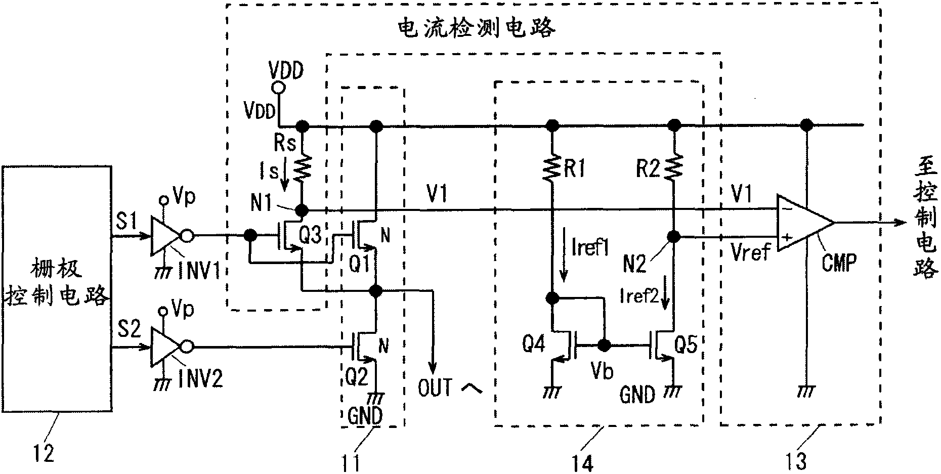
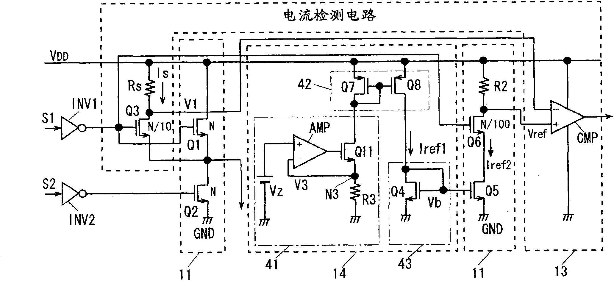
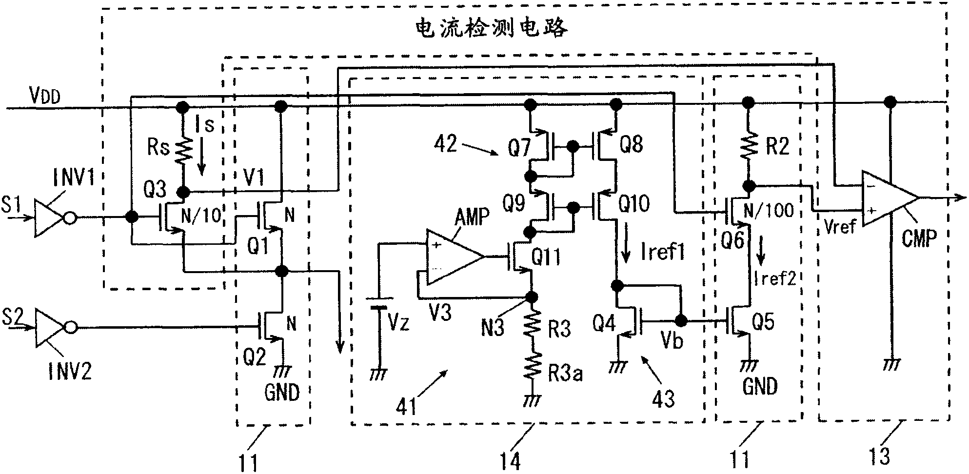
[0037] figure 1 12 shows a first embodiment of a transmission circuit built in an HBS driver / receiver IC that is implemented in a device constituting a system to which the HBS (Home Bus System) is applied and that is in charge of a communication function between devices. figure 1 The one circuit that drives one line in the twisted pair is shown in the figure. In the actual IC transmission circuit, in order to output signals with different polarities encoded by AMI, another figure 1 circuit like that.

[0038] The transmission circuit of the present embodiment includes output transistors Q1 and Q2 connected in series between the power supply voltage terminal VDD and the ground potential point GND as a push-pull type output circuit that outputs an AMI-encoded data signal by driving a transmission line. The output drive circuit 11; the gate control circuit 1...


PUM


Abstract

The present invention provides an output current detecting circuit capable of suppressing the power loss in a sensing resistor and thereby suppressing the rise of a chip temperature and a transmission circuit equipped with the output current detecting circuit. The output current detecting circuit includes: a current detecting transistor having a size smaller than that of an output transistor and a control terminal, to which a voltage same as a control voltage of the output transistor is applied; a sensing resistor connected to the current detecting transistor in a serial mode; a comparison circuit comparing a voltage converted by the sensing resistor and a reference voltage to judge a magnitude of a current flowing through the output transistor; and a reference voltage generating circuit, wherein the reference voltage generating circuit includes a constant current circuit flowing a constant current and a resistance element having one terminal connected to a power source voltage terminal, the reference voltage generating circuit generating the reference voltage based on a power source voltage by the conversion of the constant current into a voltage by flowing the constant current through the resistance element.

Description

technical field [0001] The present invention relates to an output current detection circuit with less power loss, and more particularly, to an output current detection circuit that is less affected by changes in power supply voltage or temperature, and a transmission circuit including the output current detection circuit. Background technique [0002] As a communication standard between home appliances, there is HBS (Home Bus System). In HBS, a twisted-pair (twisted-pair) is used as a transmission path, and a signal encoded by AMI (Alternate Mark Inversion) (hereinafter referred to as an AMI signal) is used in the transmission of digital signals on this transmission path. transmission. The AMI signal consists of three values ​​of zero, positive, and negative. In communication using this signal, data is transmitted by expressing logic "0" with zero and alternately changing the polarity to express logic "1". Therefore, the transmission waveform is close to an AC signal, and ...

Claims


Application Information

Patent Timeline
Patent Type & Authority Applications(China)
IPC IPC(8): H02M3/155G01R19/00
CPCG05F1/573
Inventor 大原智光后藤卓史
Owner MITSUMI ELECTRIC CO LTD
Why Eureka
Try Eureka