Photoresist removing method

A technology of photoresist and photoresist layer, applied in photosensitive material processing, electrical components, semiconductor/solid-state device manufacturing, etc., can solve the problem of ineffective removal of photoresist and polymer, lower device reliability, and poor effect etc. to avoid color difference defects, weaken damage, and improve removal effect

Inactive Publication Date: 2011-05-25
CSMC TECH FAB1 +1
View PDF1 Cites 10 Cited by
  • Summary
  • Abstract
  • Description
  • Claims
  • Application Information

AI Technical Summary

Problems solved by technology

The chromatic aberration defect after removing the photoresist is mainly caused by the adhesion of the residual photoresist and the polymer (polymer) generated during the etching process on the wafer surface. Such defects will affect the subsequent process steps, thereby reducing the reliability of the device. reliability
In the prior art, the surface of the wafer is often cleaned after ashing to remove the photoresist, but the actual effect is not good, and the residual photoresist and polymer cannot be effectively removed

Method used


Image

  • Photoresist removing method
  • Photoresist removing method
  • Photoresist removing method

Examples


Embodiment Construction

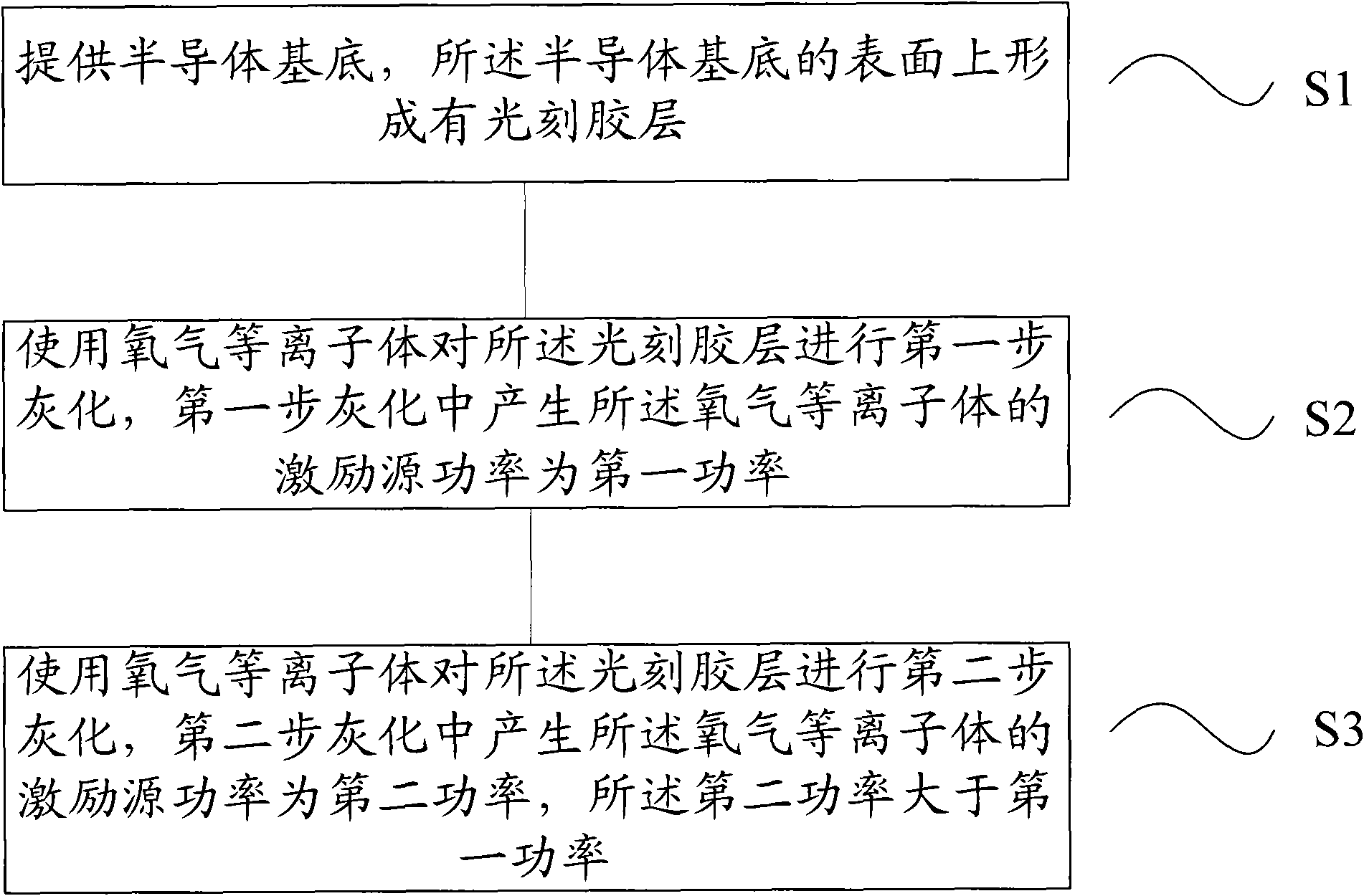
[0024] In order to make the above objects, features and advantages of the present invention more comprehensible, specific implementations of the present invention will be described in detail below in conjunction with the accompanying drawings.

[0025] In the following description, specific details are set forth in order to provide a thorough understanding of the present invention. However, the present invention can be implemented in many other ways than those described here, and those skilled in the art can make similar extensions without departing from the connotation of the present invention. Accordingly, the present invention is not limited to the specific embodiments disclosed below.

[0026] In the prior art, in order to avoid damage to the dielectric layer under the photoresist layer, the power of the excitation source for generating the oxygen plasma is often low, thereby weakening the bombardment effect of the oxygen plasma and avoiding damage. However, the inventors...


PUM


Abstract

The invention relates to a photoresist removing method comprising the following steps of: providing a semiconductor substrate, wherein a photoresist layer is formed on the surface of the semiconductor substrate; carrying out first-step ashing on the photoresist layer by using an oxygen plasma, wherein the excitation source power of the oxygen plasma generated in the first-step ashing is a first power; and carrying out second-step ashing on the photoresist layer by using the oxygen plasma, wherein the excitation source power of the oxygen plasma generated in the second-step ashing is a second power, and the second power is larger than the first power. The photoresist removing method improves the photoresist removing effect and eliminates the chromatic aberration defect.

Description

technical field [0001] The invention relates to the field of semiconductor manufacturing, in particular to a method for removing photoresist. Background technique [0002] Photolithography is one of the important process methods in the semiconductor manufacturing process, which usually includes the following steps: spin-coating photoresist on the semiconductor wafer to form a photoresist layer; selectively exposing the photoresist layer, and developing The step makes the exposed photoresist layer further form a photoresist pattern, and this step is also called patterning of the photoresist layer; using the patterned photoresist layer as a mask, the semiconductor wafer is Etching: after the etching is completed, the photoresist layer is ashed to remove the photoresist layer. [0003] The ashing process generally uses an excitation source to dissociate gases such as oxygen, so that gas molecules are ionized to generate oxygen containing oxygen or oxygen ions (O + ), and then...

Claims


Application Information

Patent Timeline
Patent Type & Authority Applications(China)
IPC IPC(8): G03F7/42H01L21/311
Inventor 肖玉洁朱旋谢宝强杨兆宇
Owner CSMC TECH FAB1
Why Eureka
Try Eureka