LDMOS (laterally diffused metal oxide semiconductor), semiconductor device integrated with same and manufacturing method thereof
A manufacturing method and semiconductor technology, applied in the direction of semiconductor/solid-state device manufacturing, semiconductor devices, electrical components, etc., can solve the complex manufacturing process of LDMOS, the on-resistance and withstand voltage can not meet the application requirements, and the difficulty of integrating IGBT and other devices, etc. problems, to achieve the effects of short production cycle, reduced on-resistance, and easy integration
Inactive Publication Date: 2011-06-15
SHENZHEN CHIP HOPE MICRO ELECTRONICS LTD
View PDF5 Cites 17 Cited by
- Summary
- Abstract
- Description
- Claims
- Application Information
AI Technical Summary
Problems solved by technology
The technical problem to be solved by the present invention is that the on-resistance and withstand voltage of LDMOS in the prior art do not meet the application requirements, devices such as IGBTs with small on-resistance are not easy to integrate, and the manufacture of LDMOS with low on-resistance For the defect of complex process, a kind of LDMOS with low on-resistance and high withstand voltage, easy to integrate and simple manufacturing process, a semiconductor device integrating the LDMOS and its manufacturing method are provided
Method used
View moreImage
Smart ImageViewing Examples

Examples
Embodiment Construction
Login to View More PUM
 Abstract
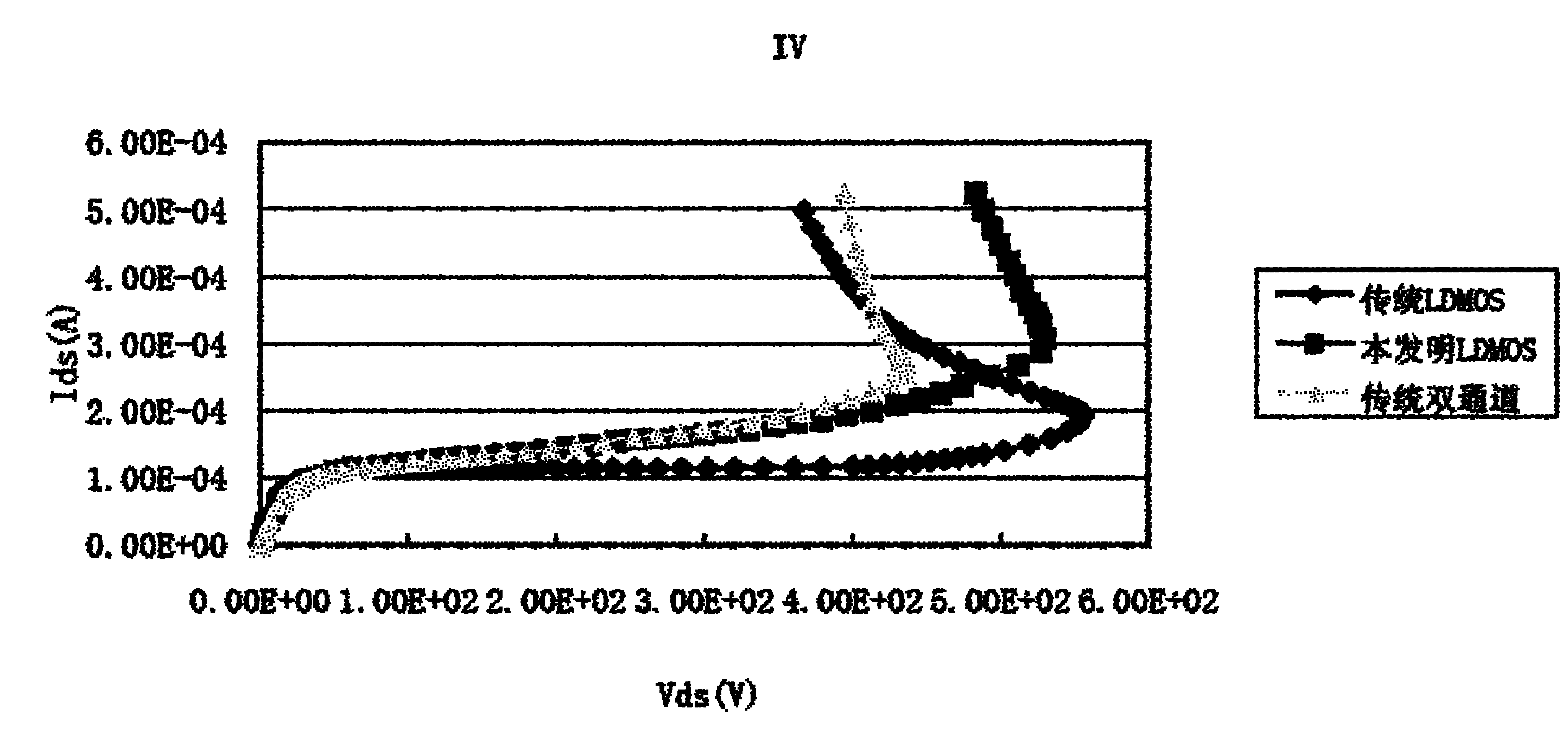
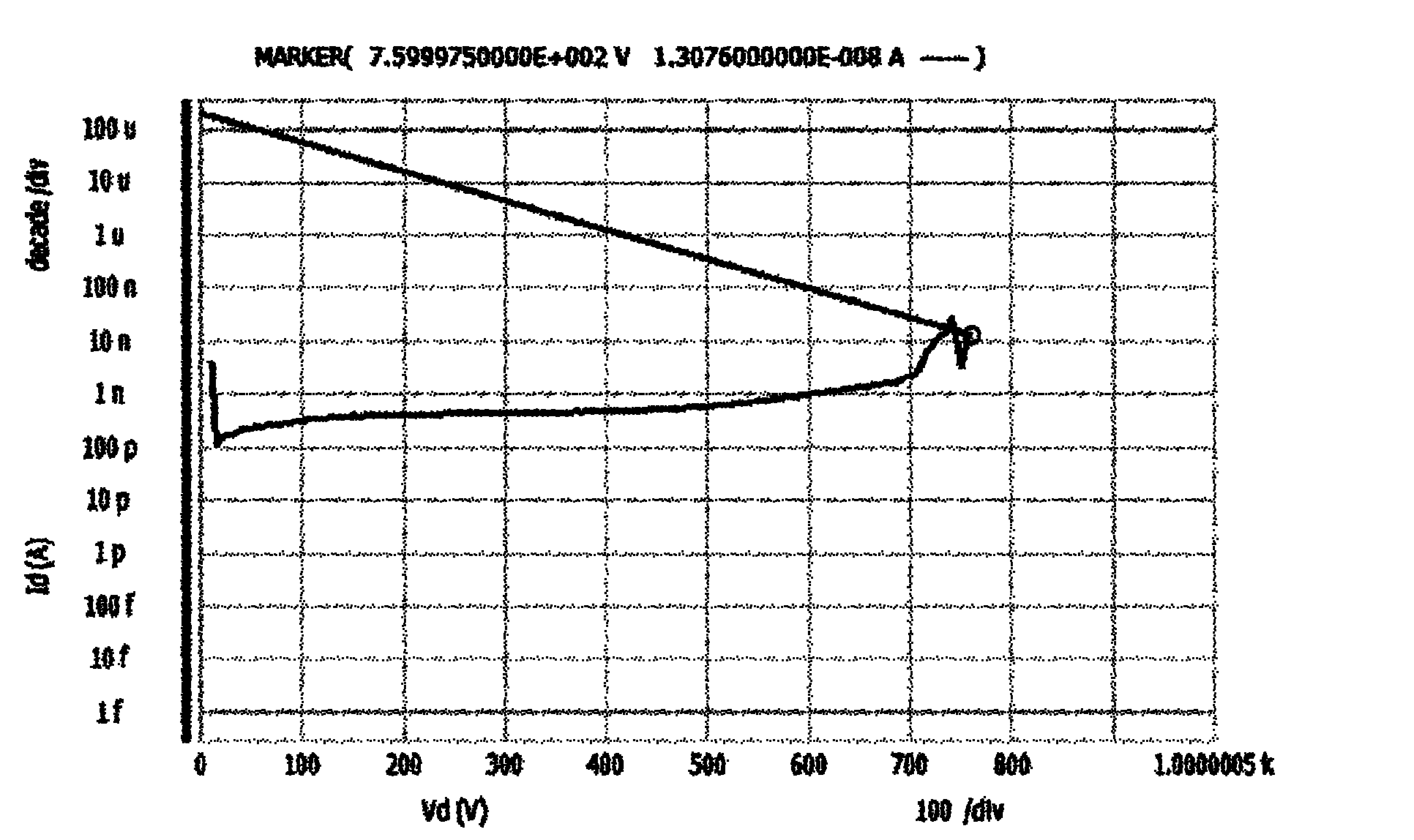
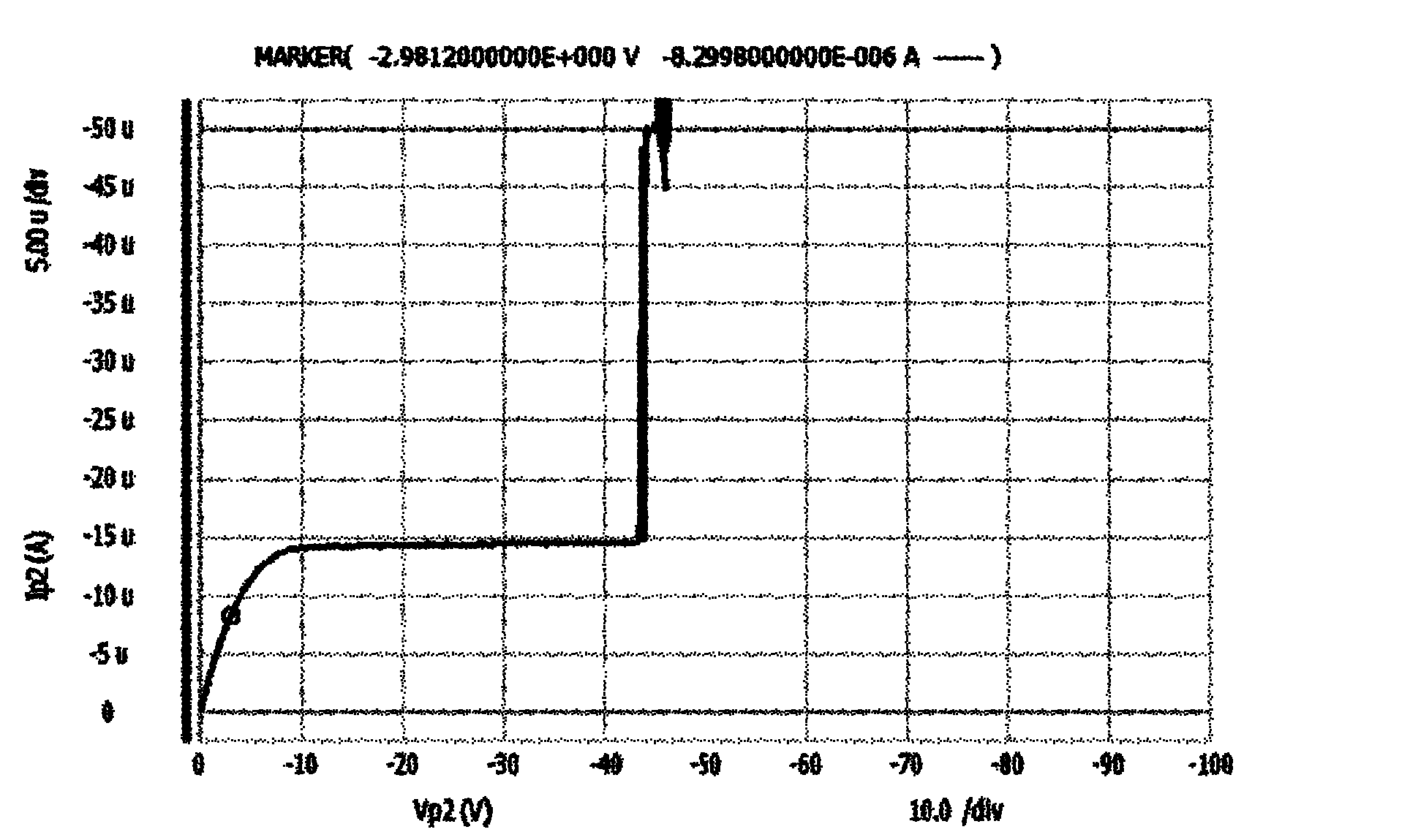
The invention discloses an LDMOS (laterally diffused metal oxide semiconductor), a semiconductor device integrated with the LDMOS and a manufacturing method thereof. The semiconductor device comprises an LDMOS 1, a CMOS (complementary metal oxide semiconductor) 2, an NPN 3 and a buried channel resistor 4 which are arranged in a P type substrate 10. The LDMOS 1 comprises an N type drift region 20, a P+ well contact region 40, a P type body region 70, an N+ source region 50, an N+ drain region 60, a gate dielectric layer 100, a source metal 80, a drain metal 90, a field oxidation layer 110 and a metal front medium 120 as well as a P type field reducing layer 30A and at least one P type buried well 30B, wherein no gap is kept between the N type drift region 20 and the P type body region, the P type buried well 30B is arranged below the P type body region 70 and is contacted with the P type body region 70, the P type field reducing layer 30A is arranged below the field oxidation layer 110 and is surrounded by the N type drift region, and a gap is kept between the P type filed reducing layer 30A and the field oxidation layer 110. The LDMOS in the invention has low on resistance and high withstand voltage and is easy to integrate, and the whole manufacturing process of the semiconductor device has simple steps and has low requirement to equipment.
Description
A kind of LDMOS, semiconductor device integrating the LDMOS and its manufacturing method technical field The invention relates to the technical field of semiconductor power devices, in particular to an LDMOS, a semiconductor device integrating the LDMOS and a manufacturing method thereof. Background technique With the rapid development of microelectronics technology, high-voltage BCD technology has been widely used in analog circuit fields such as LED drivers and switching power supplies. Among them, the power tube mainly adopts LDMOS (Lateral Double-diffused MOSFET, lateral double-diffused MOS device), and reducing its specific on-resistance (on-resistance × area) under the premise of meeting its withstand voltage requirements has become the main direction of high-voltage BCD process development. Traditional LDMOS uses single resurf (reduced surface field, reduced surface field technology) or double resurf. With the rapid development of modern analog circuits, this struct...
Claims
Login to View More Application Information
Patent Timeline
 Patent Type & Authority Applications(China)
IPC IPC(8): H01L21/8249H01L29/78H01L21/336
Inventor 毛焜乔明
Owner SHENZHEN CHIP HOPE MICRO ELECTRONICS LTD