Semiconductor structure and manufacture method thereof

A manufacturing method and semiconductor technology, applied in the fields of semiconductor/solid-state device manufacturing, semiconductor devices, electrical components, etc., can solve the problem of reducing the switching speed of components, improving on-resistance, difficult to achieve high breakdown voltage and low on-resistance at the same time, etc. problem, to achieve the effect of reducing the on-resistance and increasing the breakdown voltage

Active Publication Date: 2011-06-15
VANGUARD INTERNATIONAL SEMICONDUCTOR CORPORATION
View PDF1 Cites 12 Cited by
  • Summary
  • Abstract
  • Description
  • Claims
  • Application Information

AI Technical Summary

Problems solved by technology

However, it has been found that when the LDMOS with the above-mentioned structure is turned off, the electric field will be concentrated near the N+ type drain region 406, and the crowded electric field (or current crowding effect) will cause the breakdown voltage of the device to drop. , and at the same time reduce the switching speed of the component (switchingspeed)
On the other hand, although the method of reducing the doping concentration of the N-type well 41

Method used


Image

  • Semiconductor structure and manufacture method thereof
  • Semiconductor structure and manufacture method thereof
  • Semiconductor structure and manufacture method thereof

Examples


Example Embodiment

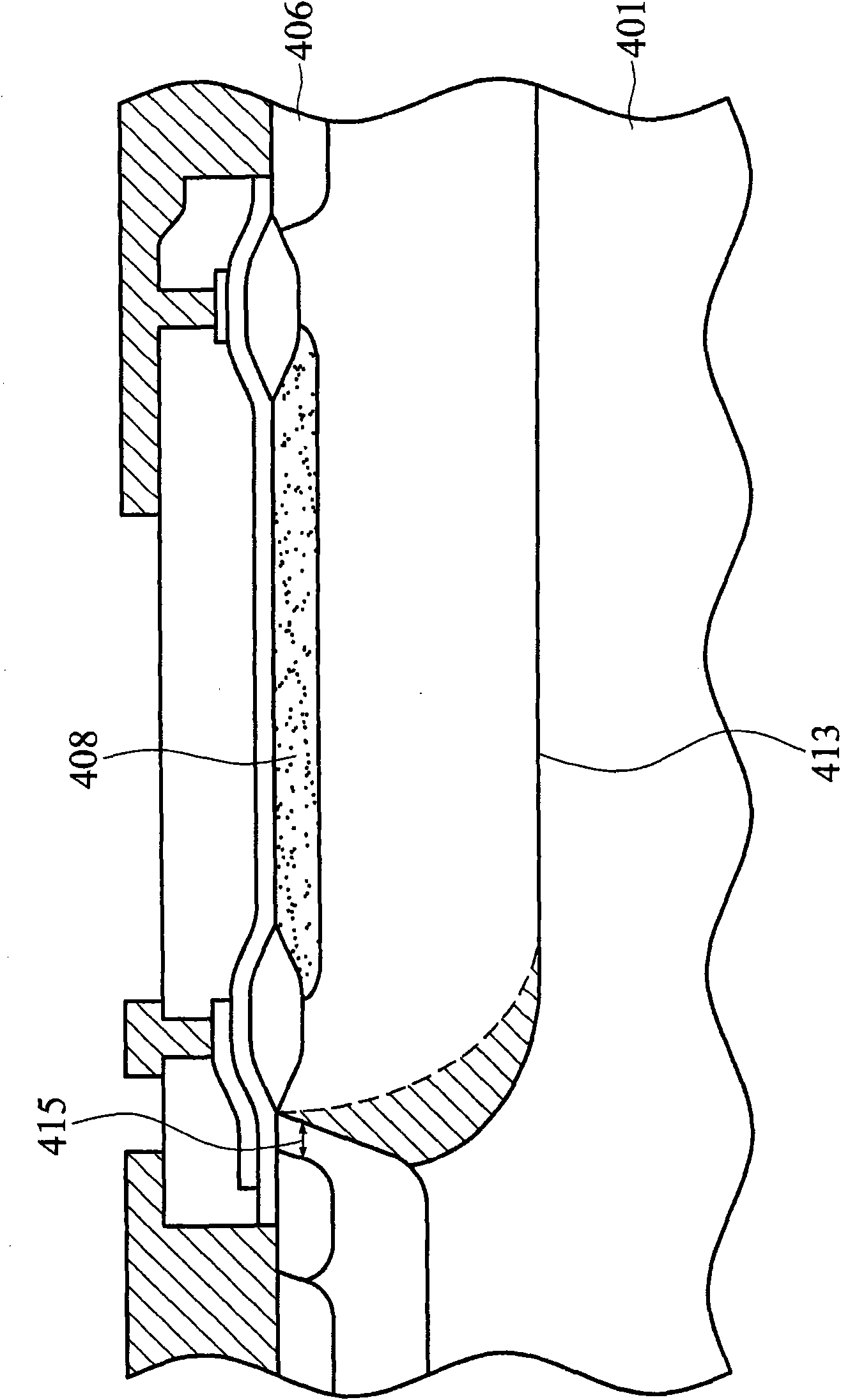
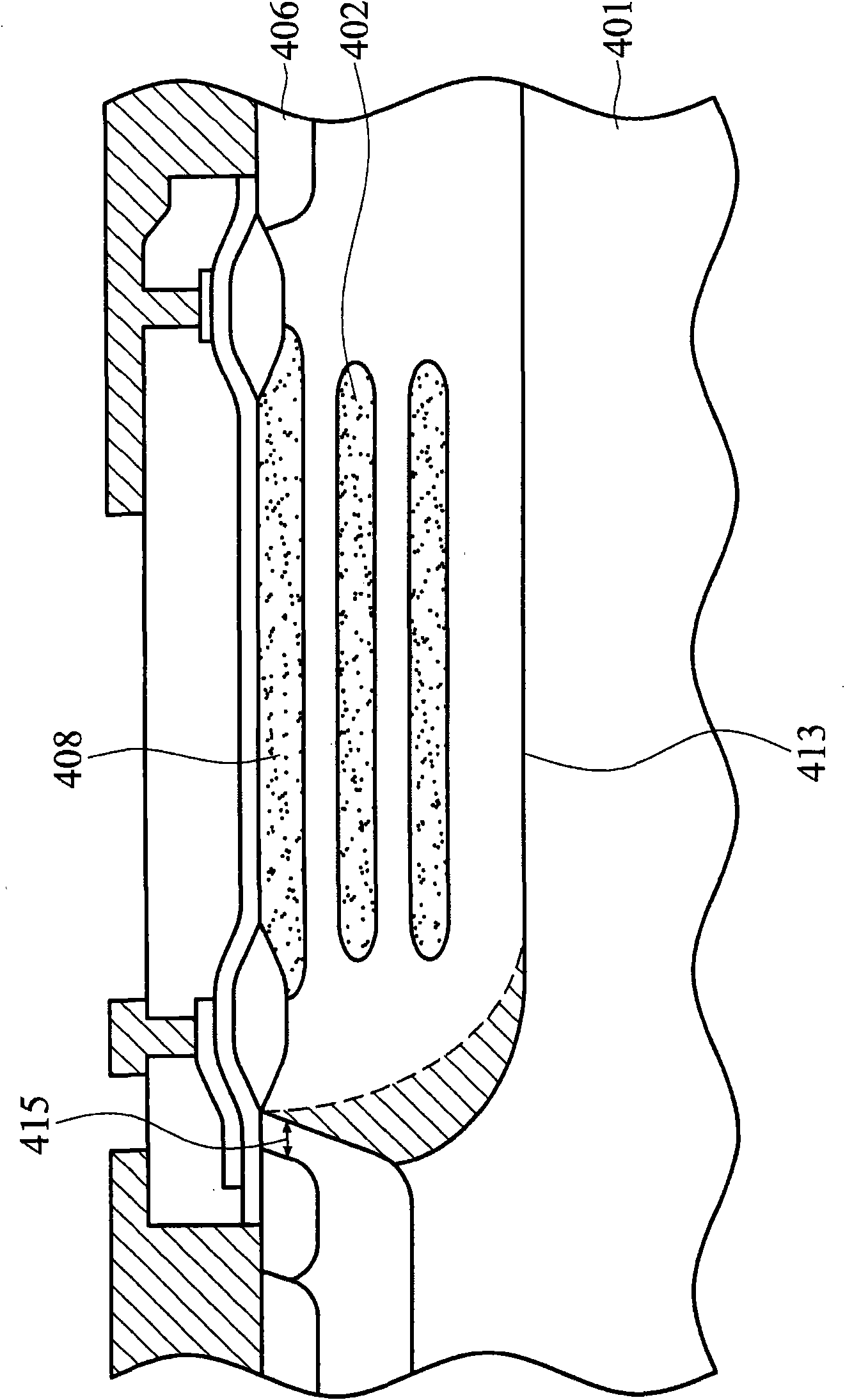
[0013] Embodiments of the present invention provide a semiconductor device and a manufacturing method thereof. The manufacturing method and use method of each embodiment are described in detail below, and will be described with accompanying drawings. Wherein, the same element numbers used in the drawings and the specification indicate the same or similar elements. In the drawings, for clarity and convenience of description, the shapes and thicknesses of the relevant embodiments may be inconsistent with reality. The following description specifically focuses on the various components of the device of the present invention or their integration. However, it should be noted that the above components are not particularly limited to those shown or described, but are known to those skilled in the art. In various forms, in addition, when a layer of material is located on another material layer or substrate, it may be directly located on its surface or other interposing layers may be a...


PUM


Abstract

The invention discloses a semiconductor structure and a manufacture method thereof. The semiconductor structure comprises a first conductive substrate, a second conductive well area, a grid electrode structure, a second conductive diffusion source electrode, a second conductive diffusion drain electrode and a plurality of first conductive buried rings, wherein the second conductive well area is arranged on the first conductive substrate; the grid electrode structure comprises a first edge and a second edge; the first edge is arranged on the second conductive well area; the second conductive diffusion source electrode is arranged on the first conductive substrate at the outer side of the second edge; the second conductive diffusion drain electrode is arranged on the second conductive well area at the outer side of the first edge; the plurality of first conductive buried rings are transversally arranged and mutually separated in the second conductive well area, and the doping outlines of the first conductive buried rings are gradually reduced from the second conductive diffusion source electrode to the second conductive diffusion drain electrode. The semiconductor structure and the manufacture method thereof, which are provided by the embodiment of the invention, can simultaneously increase the breakdown voltage and decrease the on-resistance.

Description

technical field [0001] The invention relates to a semiconductor structure and a manufacturing method thereof, in particular to a double-diffused metal oxide semiconductor transistor and a manufacturing method thereof, so as to increase breakdown voltage and reduce on-resistance at the same time. Background technique [0002] In today's integrated circuit manufacturing process, a large number of devices such as controllers, memories, low-voltage operating elements, and high-voltage power elements have been integrated in a single chip, thus forming a single chip system. In order to cope with high voltage and current requirements, high voltage devices such as double-diffused metal oxide semiconductor (DMOS) transistors are usually used in power supply devices, which have low conduction when operating at high voltages. Resistance (on-resistance). In addition, other high-voltage devices such as laterally diffused metal oxide semiconductor transistors (Lateral double-diffused met...

Claims


Application Information

Patent Timeline
IPC IPC(8): H01L29/78H01L29/06H01L21/336
CPCH01L29/7816H01L29/42368H01L29/0634
Inventor 张义昭杜尚晖许健
Owner VANGUARD INTERNATIONAL SEMICONDUCTOR CORPORATION
Why Eureka
Try Eureka