Schottky diode structure for reducing reverse leakage current by utilizing generated depletion area

A technology of Schottky diodes and depletion regions, applied in the field of diodes

Inactive Publication Date: 2011-06-15
PYNMAX TECH
View PDF0 Cites 2 Cited by
  • Summary
  • Abstract
  • Description
  • Claims
  • Application Information

AI Technical Summary

Problems solved by technology

[0003] From another point of view, when a reverse voltage is applied, it can be found that the reverse leakage current of the Schottky diode is significantly higher than that of the P-N junction diode. This is the shortcoming of the Schottky diode, but it is currently lacking in high current density or low current The forward voltage drop generated by the density can maintain the advantage of high-speed operation, and reduce the reverse leakage current Schottky diode under the reverse voltage

Method used


Image

  • Schottky diode structure for reducing reverse leakage current by utilizing generated depletion area
  • Schottky diode structure for reducing reverse leakage current by utilizing generated depletion area
  • Schottky diode structure for reducing reverse leakage current by utilizing generated depletion area

Examples


Embodiment Construction

[0018] The Schottky diode structure of the present invention has semiconductor materials, which are described as "first conductive material" and "second conductive material" in the following description, wherein, if the first conductive material is a P-type semiconductor material, then The second conductive material is an N-type semiconductor material; otherwise, if the first conductive material is an N-type semiconductor material, the second conductive material refers to a P-type semiconductor material.

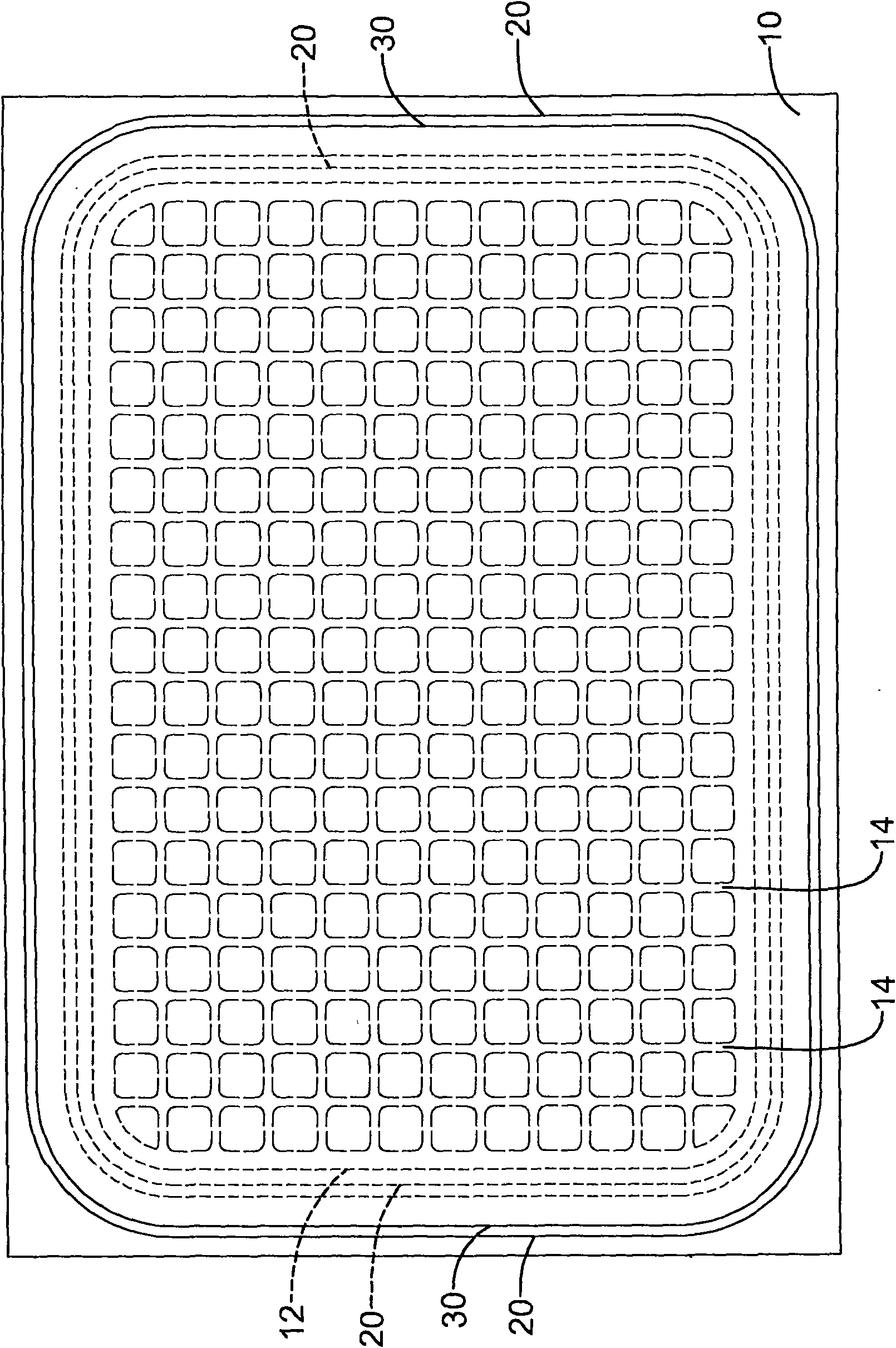
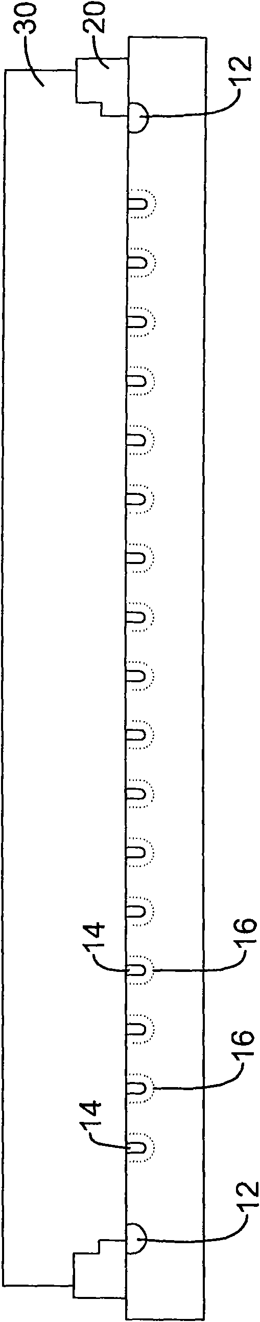
[0019] Please refer to figure 1 , 2 As shown, it is a schematic plan view and a schematic cross-sectional view of the first embodiment of the present invention, including:

[0020] A first conductive material semiconductor substrate 10, a substrate made of a first conductive material semiconductor material, for example, an N-type substrate can be formed with pentavalent materials such as arsenic and phosphorus, on the periphery of the first conductive material semiconducto...


PUM


Abstract

The invention relates to a Schottky diode structure for reducing a reverse leakage current by utilizing a generated depletion area, provided with a first conductive material semiconductor substrate and a metal layer combined with the same. The combined periphery of the first conductive material semiconductor and the metal layer is provided with an oxide layer, wherein a plurality of linearly arranged second conductive material areas are formed in the surface of the first conductive material semiconductor substrate, adjacent to the metal layer, and the second conductive material regions can form a depletion area in the first conductive material semiconductor substrate so that the depletion area can reduce the electric leakage area of a Schottky diode and further decrease the reverse leakage current and the forward voltage drop of the Schottky diode. When the first conductive material is a P-type semiconductor, a second conductive material is an N-type semiconductor; and on the contrary, and when the first conductive material is a N-type semiconductor, the second conductive material is a P-type semiconductor.

Description

technical field [0001] The present invention relates to a diode, especially a Schottky that forms a linearly distributed second conductive material region inside a first conductive material semiconductor substrate to generate a depletion region to reduce reverse leakage current and forward voltage drop diode structure. Background technique [0002] Please refer to Figure 5 As shown, the characteristic curve A shown in the figure is a general P-N junction diode, and the other curve B is the characteristic curve of a general Schottky diode. Among them, when the current applied to the diode is a forward current, it can be seen that the forward voltage drop of the P-N junction diode is higher than that of the Schottky diode in the range where the forward current is small, but the general P-N junction diode When the forward current applied to its components increases, the forward voltage drop of its components will be smaller than the forward voltage drop of the Schottky diode ...

Claims


Application Information

Patent Timeline
Patent Type & Authority Applications(China)
IPC IPC(8): H01L29/872H01L29/06
CPCH01L29/872H01L29/0692H01L29/0619
Inventor 童钧彦陈坤贤王凯莹沈宜蓁翁宏达
Owner PYNMAX TECH
Why Eureka
Try Eureka