Optoelectronic semiconductor device

A technology of optoelectronic semiconductors and optoelectronic devices, applied in the direction of semiconductor devices, semiconductor lasers, lasers, etc., can solve the problems of GaN high thermal expansion mismatch, unavailability, expensive large wafer size, etc.

Inactive Publication Date: 2011-06-15
QUNANO
View PDF3 Cites 8 Cited by
  • Summary
  • Abstract
  • Description
  • Claims
  • Application Information

AI Technical Summary

Problems solved by technology

Likewise, these materials also suffer from the high thermal expansion mismatch of GaN
Moreover, SiC and AL 2 o 3 are expensive and large wafer sizes are still not commercially available

Method used


Image

  • Optoelectronic semiconductor device
  • Optoelectronic semiconductor device
  • Optoelectronic semiconductor device

Examples


Embodiment Construction

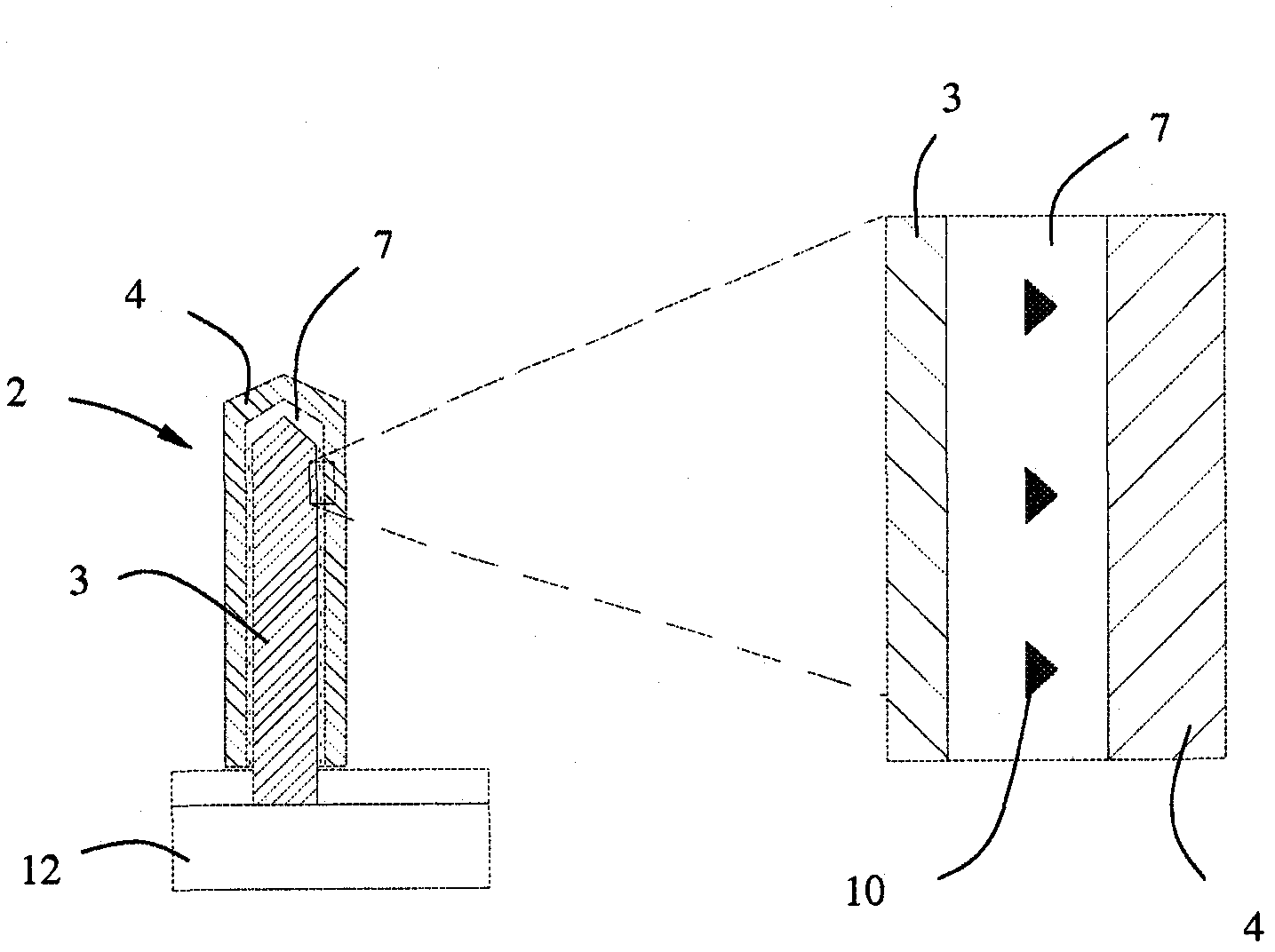
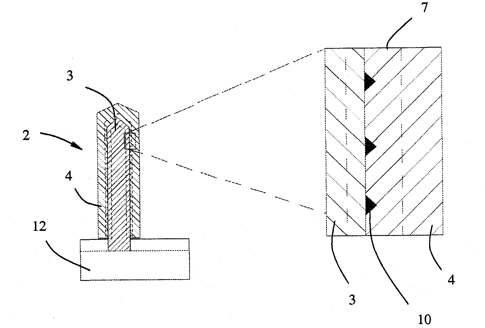
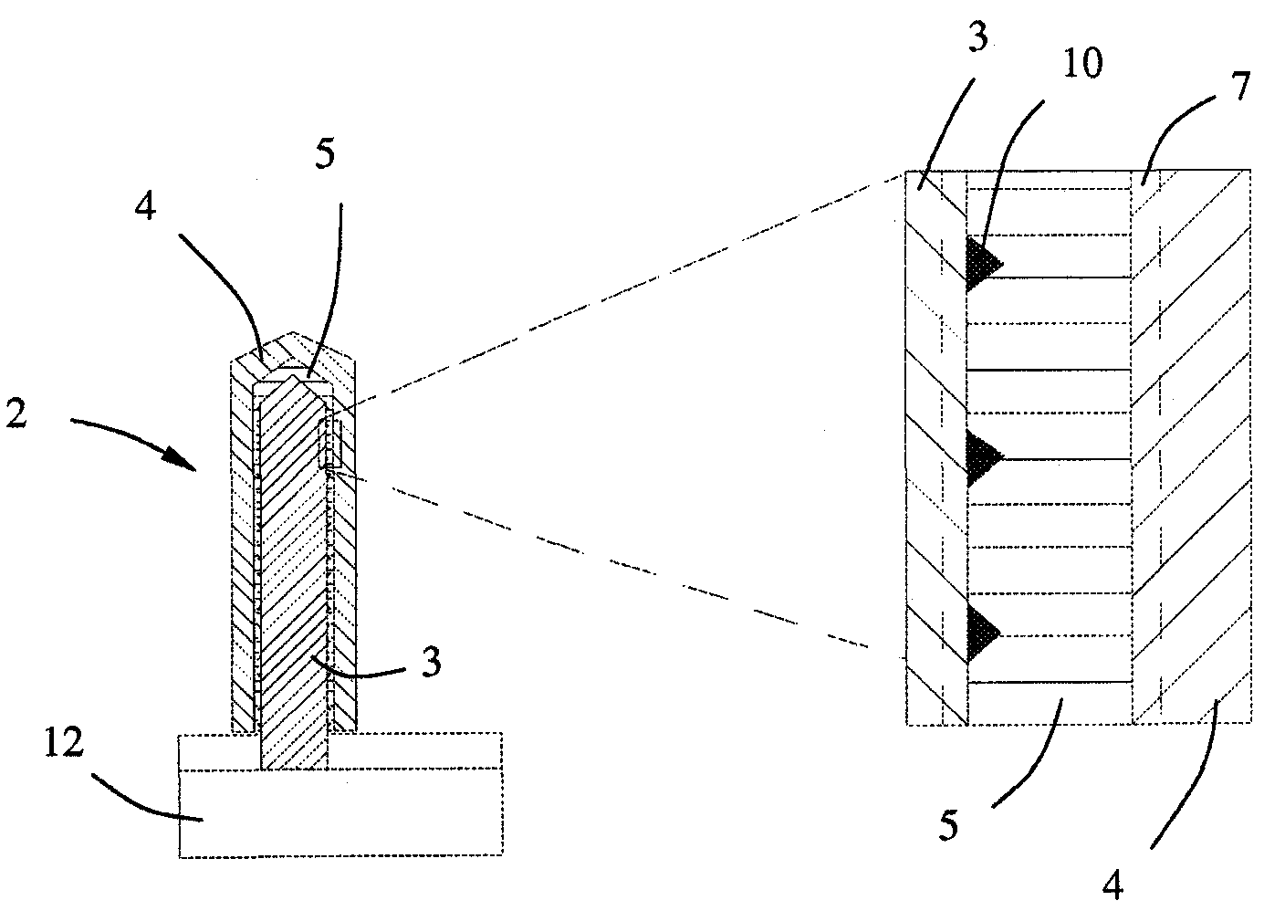
[0025] Nanowires are generally interpreted as nanostructures whose diameters are nanometer-sized. As the term "nanowire" implies, its lateral dimensions are on the order of nanometers and its longitudinal dimensions are unlimited. Such nanostructures are also commonly referred to as nanowhiskers, one-dimensional nanocomponents, nanorods, and the like. Although these terms imply an elongated shape, the nanowires may be tapered or stub-like, and since nanowires may have a variety of cross-sectional shapes, in this application the diameter is intended to mean effective diameter. Generally, nanowires are considered to have at least two dimensions, each no larger than 300 nm, but nanowires may have a diameter or width of up to about 1 um. The one-dimensional nature of the nanowires provides unique physical, optical and electronic properties. These properties can be used, for example, to form devices that exploit quantum mechanical effects or to form heterostructures of compositi...


PUM


Abstract

The present invention provides an optoelectronic semiconductor device comprising at least one semiconductor nanowire (2), wherein the nanowire (2) comprises a nanowire core (3) and at least one shell layer (4) arranged around at least a portion of the nanowire core (3). The nanowire core (3) and the shell layer (4) form a pn or pin junction that in operation provides an active region (7) for carrier generation or carrier recombination. Quantum dots (10) adapted to act as carrier recombination centres or carrier generation centres are arranged in the active region (7). By using the nanowire core (3) as template for formation of the quantum dots (10) and the shell layer (4), quantum dots of homogeneous size and uniform distribution can be obtained. Basically, the optoelectronic semiconductor device can be used for light generation or light absorption. In the former case the optoelectronic semiconductor device is a light emitting diode or a laser diode and in the latter case the optoelectronic semiconductor device is a photoelectric device, such as a photo diode, a photo detector or a solar cell.

Description

technical field [0001] The present invention relates to the use of self-assembled quantum dots (and in particular Stranski Krastanow dots) in optoelectronic semiconductor devices such as light emitting diodes and optoelectronic devices. Background technique [0002] Self-assembled quantum dots, or Stranski Krastanow dots (hereinafter interchangeably referred to as SK dots or simply quantum dots) are used as efficient one-dimensional quantum wells in semiconductor devices. These quantum dots have been realized in a large number of semiconductor material systems, such as InAs / GaAs, InAs / InP, InP / GaAs, InGaN / GaN, InN / GaN, GaN / AlGaN, etc., grown on planar surfaces or along edges. [0003] The semiconductor quantum dots may be formed during epitaxial growth of a semiconductor layer on a substrate that is lattice mismatched to the semiconductor layer. During this growth, point formation is promoted by minimizing the energy associated with crystallographic strain. The size of the...

Claims


Application Information

Patent Timeline
Patent Type & Authority Applications(China)
IPC IPC(8): H01L29/06H01L29/12H01L31/06H01L31/102H01L33/00
CPCH01L33/24H01L33/08H01S5/341H01L33/20H01L33/32H01L31/03529H01L31/0304H01L31/028Y02E10/544H01L31/035281B82Y20/00H01L31/0296Y02E10/547
Inventor J・奥尔松L・萨米尔松
Owner QUNANO
Why Eureka
Try Eureka