Light-emitting component and manufacturing method thereof

A technology for a light-emitting element and a manufacturing method, which is applied to electrical components, semiconductor devices, circuits, etc., can solve the problems of difficulty in improving the luminous efficiency of light-emitting diodes

Active Publication Date: 2011-06-22
EPISTAR CORP
View PDF0 Cites 10 Cited by
  • Summary
  • Abstract
  • Description
  • Claims
  • Application Information

AI Technical Summary

Problems solved by technology

[0004] However, the multiple quantum well structure layer is easily affected by carrier overflow and piezoelectric field effect, making it difficult for electrons and holes to be effectively confined in the multiple quantum well structure for combination, thus making it difficult to improve the luminous efficiency of light-emitting diodes

Method used


Image

  • Light-emitting component and manufacturing method thereof
  • Light-emitting component and manufacturing method thereof
  • Light-emitting component and manufacturing method thereof

Examples


Embodiment Construction

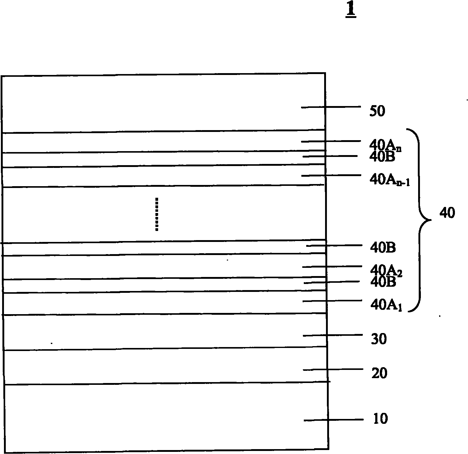
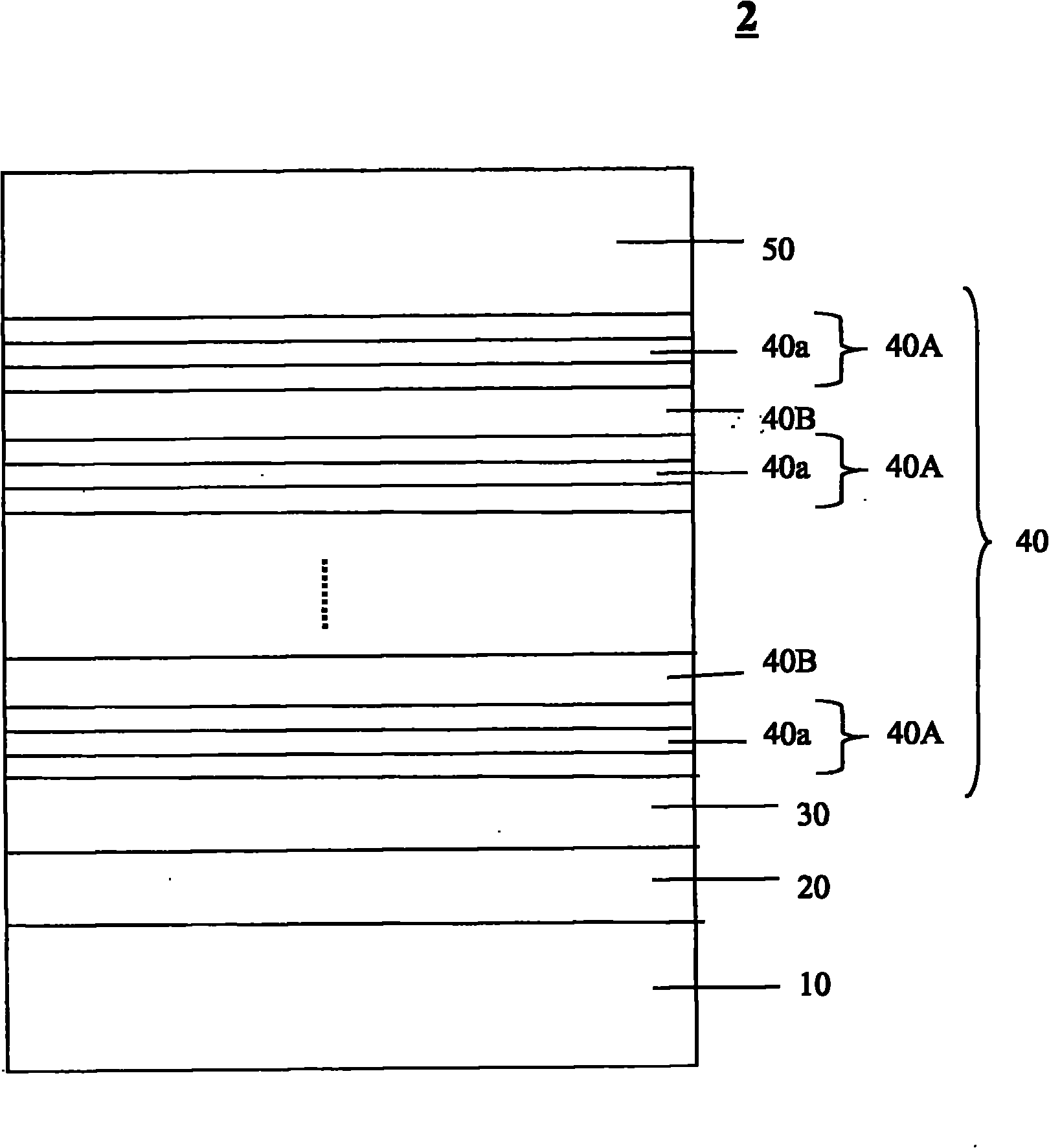
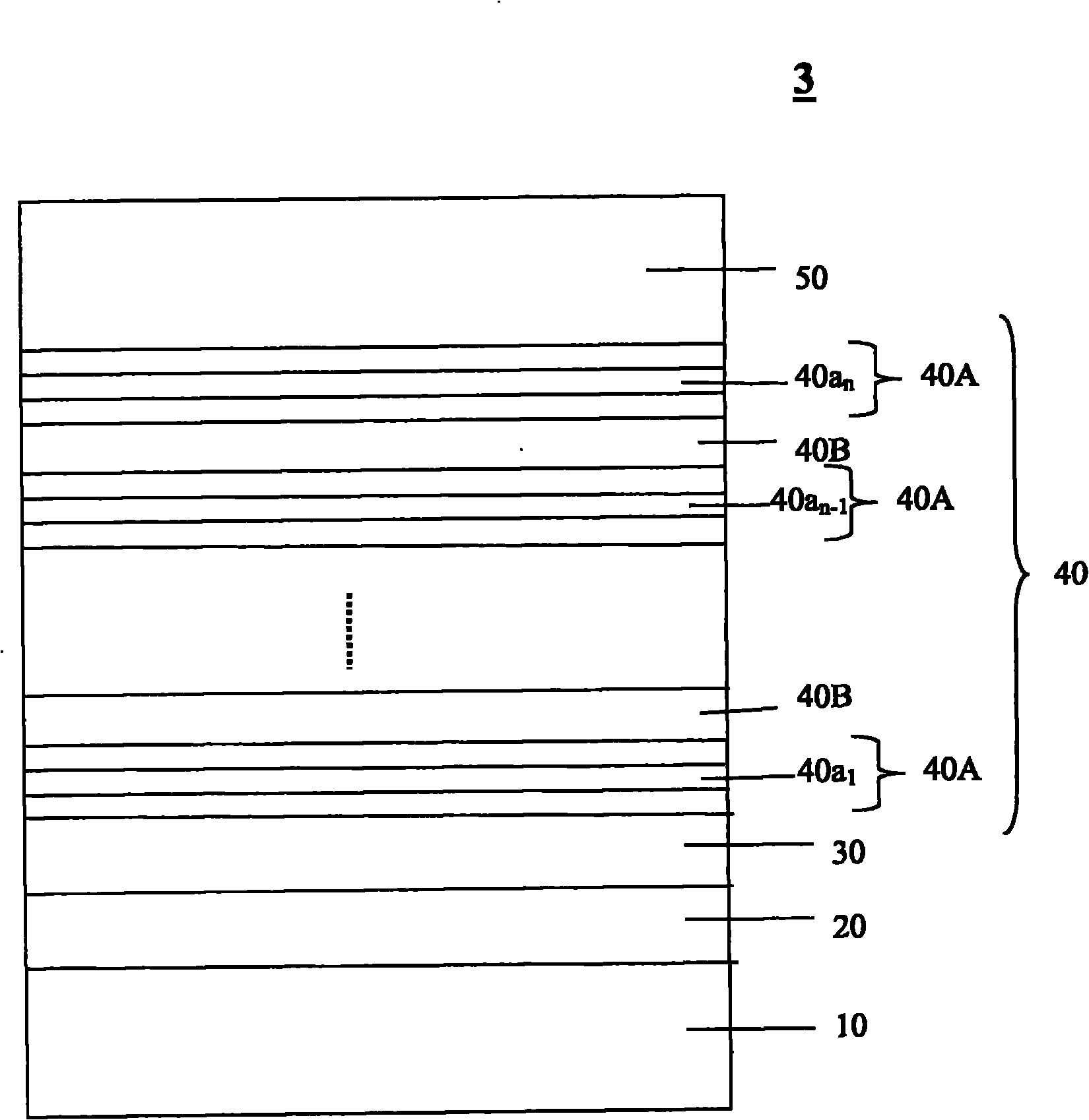
[0025] The first embodiment of the present invention discloses a light emitting device including an active layer. Its active layer is a multiple quantum well structure formed by stacking multiple barrier layers and multiple well layers alternately, in which the barrier layer is doped with p-type impurities to increase the number of holes, and the closer to the potential of the n-type bound layer The lower the doping concentration of the barrier layer, the higher the doping concentration of the barrier layer closer to the p-type bound layer, so as to form a barrier layer structure with a gradual doping concentration. In order to make the narration of this embodiment more detailed and complete, it can cooperate with figure 1 For the drawings, refer to the following description.

[0026] figure 1 A first embodiment of the epitaxial structure of the light-emitting element according to the present invention is disclosed. The epitaxial structure 1 includes a growth substrate 10, a...


PUM


Abstract

The invention relates to a light-emitting component and a manufacturing method thereof. The light-emitting component contains an n-shaped bound layer, a p-shaped bound layer and an active layer, wherein the active layer is positioned between the n-shaped bound layer and the p-shaped bound layer and in a multiple-quantum well structure formed by piling multiple barrier layers and multiple well layers in a stagger way; the barrier layers are doped with p-shaped impurities to increase the number of cavities, the barrier layers which are closer to the n-shaped bound layer have lower doping concentration, and the barrier layers which are closer to the p-shaped bound layer have higher doping concentration so as to form a barrier layer structure with gradual change type doping concentration. Thelight-emitting component can enhance the combination probability of the cavities and electrons, thereby enhancing the light-emitting efficiency.

Description

technical field [0001] The invention relates to a light-emitting element, especially a light-emitting diode element with a multiple quantum well structure. Background technique [0002] Light Emitting Diode (LED) has been widely used in automobiles, computers, communications and consumer electronics due to its small size, long life, low driving voltage, low power consumption, fast response, and good shock resistance. products etc. [0003] Generally speaking, a light emitting diode has an active layer disposed between two types of cladding layers (p-type & n-type cladding layers) of different electrical properties. When a driving current is applied to the electrodes above the two binding layers, the electrons and holes in the two binding layers will be injected into the active layer and combined in the active layer to emit light. Each surface emits. Generally, the active layer can be a single quantum well structure layer (SQW) or a multiple quantum well structure layer (M...

Claims


Application Information

Patent Timeline
Patent Type & Authority Applications(China)
IPC IPC(8): H01L33/06H01L33/26
Inventor 颜胜宏蔡孟伦蔡清富
Owner EPISTAR CORP
Why Eureka
Try Eureka