Ultrathin LED light source plate and packaging method thereof

A technology of LED light source and packaging method, applied in the direction of light source fixing, lighting device, lighting device parts, etc., can solve the problems of easy foaming, thick light source board thickness, reliability problems, etc., and achieves high reliability and weight. Light and thin effect

Inactive Publication Date: 2011-06-29
厦门亮而丽光电科技有限公司
View PDF6 Cites 7 Cited by
  • Summary
  • Abstract
  • Description
  • Claims
  • Application Information

AI Technical Summary

Problems solved by technology

This conventional glue filling method has many disadvantages: First, it is difficult to guarantee the uniformity of glue filling, which causes the light output of the light source board to fail to meet the design requirements; Meeting the design requirements also brings problems to reliability; the glue filling process is difficult to achieve a very thin glue layer, so the thickness of the LED light source board is thicker, making the thickness of the light source board thicker, and the cost of glue filling is also greatly increased; The thickness of the light source board is thicker, which also increases the cost of subsequent lamp preparation; also because the thickness of the light source board is thicker, it is difficult to divide the light source board after glue filling; the production efficiency of the glue filling process is relatively low

Method used


Image

  • Ultrathin LED light source plate and packaging method thereof
  • Ultrathin LED light source plate and packaging method thereof
  • Ultrathin LED light source plate and packaging method thereof

Examples


Embodiment 1

[0034] The encapsulation method is as follows:

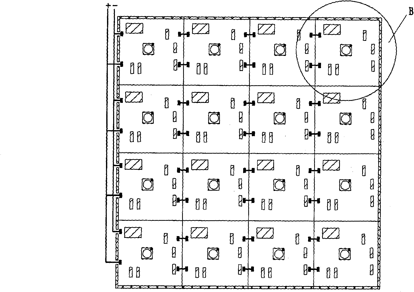
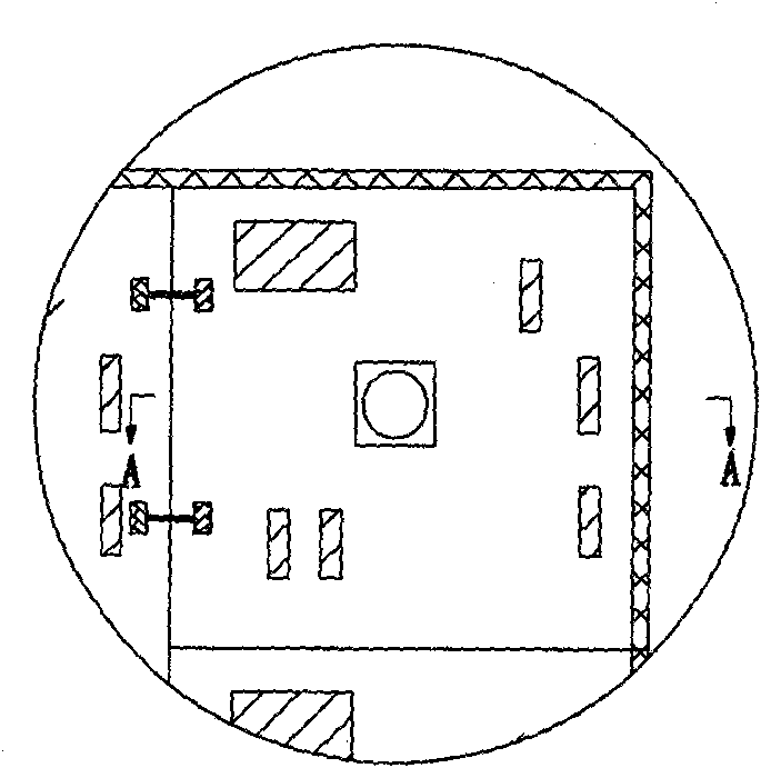
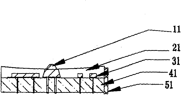
[0035] Design circuit on circuit board - circuit board cleaning - solder paste coating at soldering point - patching of electronic components such as resistors - LED light source patching - circuit board cleaning - reflow soldering - testing - laying EVA film - laying cover plate - lamination - trimming - curing - testing.

Embodiment 2

[0037] If the LED light source uses thermal paste as the heat dissipation connection, the packaging method includes the following steps:

[0038] Design circuit on the circuit board-circuit board cleaning-solder paste coating at soldering point-resistor and other electronic components placement-circuit board cleaning-reflow soldering-coating thermal paste-LED light source placement-LED light source positive and negative welding-test - Laying of EVA film - Laying of cover - Lamination - Trimming - Curing - Testing.

Embodiment 3

[0040] If plug-in electronic components and LED light sources are used, the packaging method includes the following steps:

[0041] Design jacks and circuits on the circuit board-circuit board cleaning-resistor and other electronic components plug-in and welding-LED light source plug-in and welding-circuit board cleaning-testing-laying EVA film-laying cover board-lamination-cutting-curing -test.


PUM


Abstract

The invention provides an ultrathin light emitting diode (LED) light source plate and a packaging method thereof. The packaging method comprises the following steps of: designing a circuit on a circuit board, cleaning the circuit board, welding an LED light source and an electronic component on the circuit board, testing, laying an ethylene-vinyl acetate copolymer (EVA) glue film, laying a cover plate, laminating, trimming, curing and testing. The ultrathin LED light source plate packaged by the method is characterized by being provided with the circuit board, wherein the LED light source and the electronic component are welded on the circuit board; the glue film is laid on the circuit board; the cover plate is laid on the glue film; and the circuit board, the glue film and the cover plate are laminated to form a whole. The glue film and the cover plate are laid in turn, and a laminating process is applied to the packaging of the LED light source plate, so that the LED light source plate which has higher reliability, smaller thickness, lighter weight, lower cost and more flexible applicability can be obtained.

Description

technical field [0001] The invention belongs to the field of LED light source processing, and in particular relates to an ultra-thin LED light source board and a packaging method thereof. Background technique [0002] With the vigorous development of the world's semiconductor industry and the continuous progress of industrial technology and theoretical research on light-emitting mechanisms, LEDs have rapidly been commercialized in developed countries and regions in the semiconductor industry. The high brightness of LED and the realization of all colors in the visible light band make people see the hope of the full application of new LED light sources. Experts also predict that LED light sources will replace incandescent and fluorescent lamps as a new generation of lighting sources. Compared with traditional incandescent and fluorescent lamps, LED lighting sources have huge advantages. First of all, the LED light source is small in size, long in life, and compact in structu...

Claims


Application Information

Patent Timeline
Patent Type & Authority Applications(China)
IPC IPC(8): F21V19/00H01L21/50H01L21/56H01L33/00
CPCH01L2224/97
Inventor 杨露
Owner 厦门亮而丽光电科技有限公司
Why Eureka
Try Eureka