Method for manufacturing circuit board

A circuit board production and circuit board technology, which is applied in the secondary treatment of printed circuits, coating of non-metallic protective layers, etc., can solve the problems of difficult control of micro-etching degree, circuit breakage, etc.

Active Publication Date: 2011-06-29
AVARY HLDG (SHENZHEN) CO LTD +1
View PDF0 Cites 6 Cited by
  • Summary
  • Abstract
  • Description
  • Claims
  • Application Information

AI Technical Summary

Problems solved by technology

In this way, the degree of micro-corrosion is difficult to control, and the conductive line

Method used


Image

  • Method for manufacturing circuit board
  • Method for manufacturing circuit board
  • Method for manufacturing circuit board

Examples


Embodiment Construction

[0015] The circuit board manufacturing method provided by the technical solution will be further described in detail below in conjunction with the accompanying drawings and embodiments. The circuit board manufacturing method provided by the embodiment of the technical solution includes the following steps:

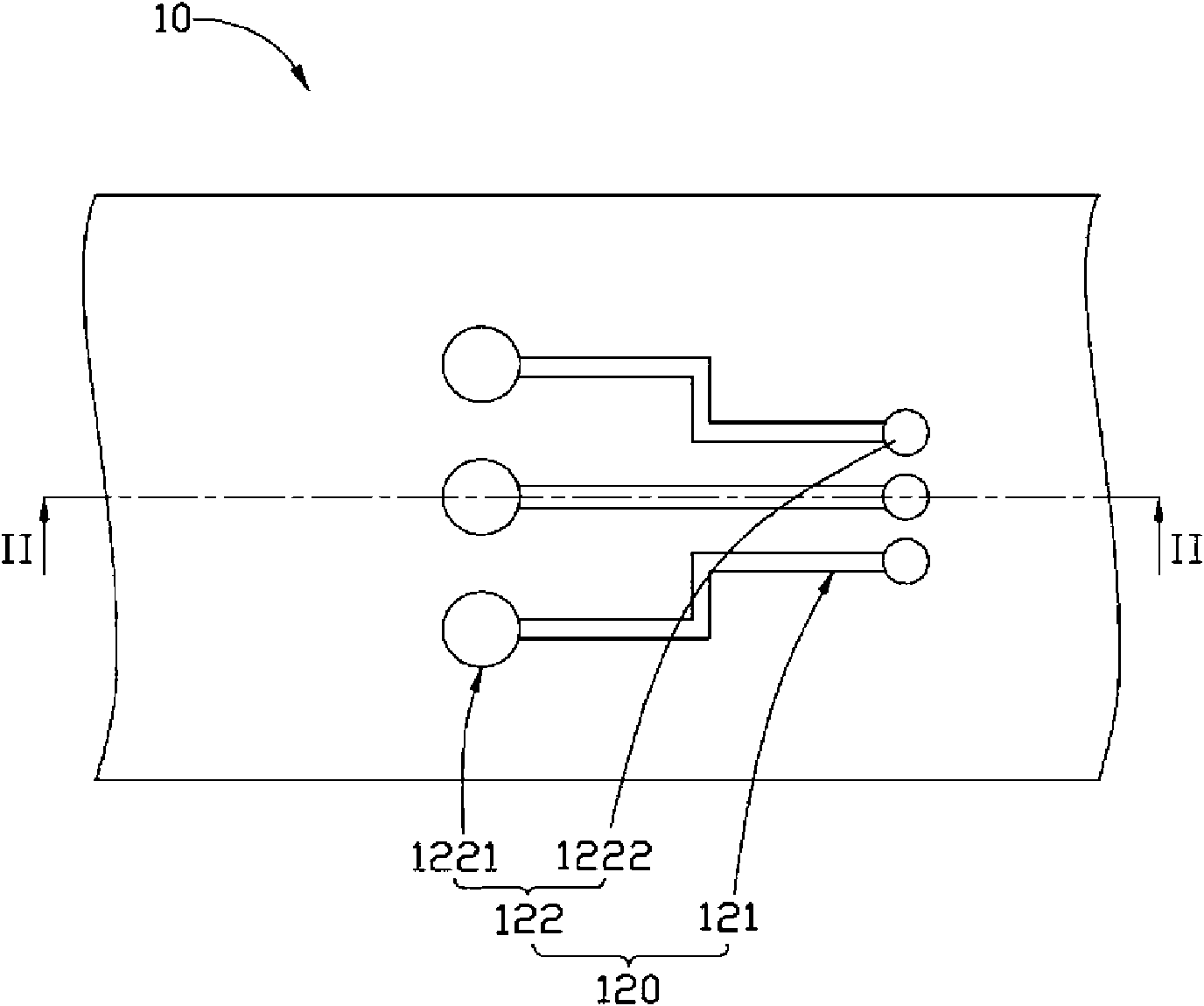
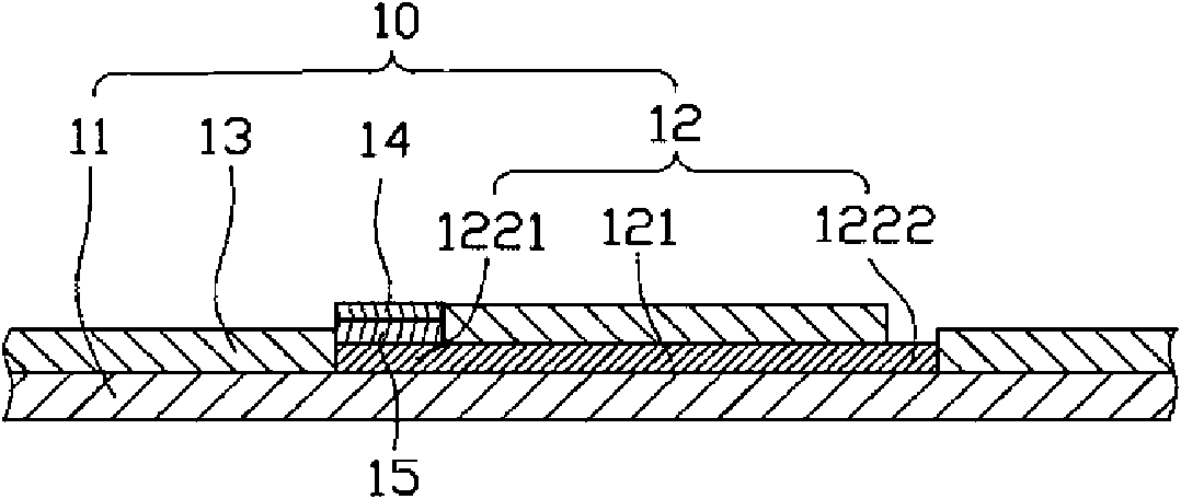
[0016] For the first step, please also refer to figure 1 and figure 2 , providing a circuit board 10 .

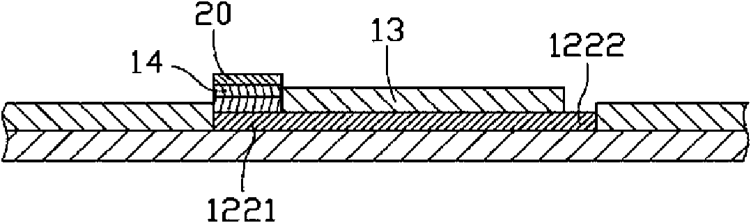
[0017] The circuit board 10 can be a multi-layer board or a single-layer board. In this embodiment, the circuit board 10 is introduced as an example of a single-layer board that has undergone processing steps such as making circuits, making a covering layer, electroless nickel plating, and electroless gold plating. The circuit board 10 includes an insulating layer 11 , a conductive layer 12 , a covering layer 13 and a plating layer 14 .

[0018] The insulating layer 11 can be a hard resin layer, such as epoxy resin, glass fiber cloth, etc., or a flexible resin laye...


PUM


Abstract

The invention provides a method for manufacturing a circuit board, which comprises the following steps of: providing the circuit board, wherein the circuit board comprises an insulating layer, a conducting layer formed on the insulating layer and a plating layer formed on part of the conducting layer; the material of the conducting layer has a first electrode potential; the plating layer is in an electric contact with the conducting layer; the material of the plating layer has a second electrode potential; the second electrode potential is greater than the first electrode potential; forming a protective layer on the plating layer; performing wet treatment on the circuit board by wet treatment liquid, wherein the wet treatment liquid is an electrolyte, and during the wet treatment process, the protective layer and at least part of the conducting layer are exposed to the wet treatment liquid; removing the protective layer to obtain the circuit board which is subjected to the wet treatment. By the method for manufacturing the circuit board provided by the technical scheme, and galvanic corrosion between the plating layer and part of the exposed conducting layer in the wet treatment liquid is avoided, so the manufacturing yield and excellent performance of the circuit board are guaranteed.

Description

technical field [0001] The invention relates to circuit board manufacturing technology, in particular to a circuit board manufacturing method. Background technique [0002] Flexible circuit boards are widely used in various fields, especially in portable electronic devices that require lightness, thinness, shortness, and smallness, such as mobile phones. Flexible printed circuit boards for mobile phones are usually produced through the steps of making circuits, making covering layers, electroless nickel plating, electroless gold plating, organic coating processes, and assembly processes. In the circuit manufacturing process, usually a plurality of conductive circuits and a plurality of pads are formed on the flexible circuit board. The plurality of conductive traces and the plurality of pads are typically copper, and each pad is connected to at least one conductive trace. The subsequent step of forming a covering layer refers to forming a covering layer on a plurality of c...

Claims


Application Information

Patent Timeline
IPC IPC(8): H05K3/28
Inventor 周琼
Owner AVARY HLDG (SHENZHEN) CO LTD
Why Eureka
Try Eureka