
Screening method for integrated circuit

A technology of integrated circuits and screening methods, applied in electronic circuit testing, non-contact circuit testing, semiconductor/solid-state device testing/measurement, etc., can solve problems such as slow inspection speed, reduced reliability, and inappropriate detection of large-sized devices. Achieve the effect of fast detection speed and automatic detection accuracy

Inactive Publication Date: 2011-07-06
上海允科自动化有限公司
View PDF3 Cites 2 Cited by
  • Summary
  • Abstract
  • Description
  • Claims
  • Application Information

AI Technical Summary

Problems solved by technology

However, these two methods have the following disadvantages in actual use: as far as online inspection is concerned, since only structural defects can be inspected and the inspection speed is slow, they are not suitable for the detection of large-scale devices on the entire wafer; For DC electronic probe testing, when the detected integrated circuit is composed of many electronic components (such as transistors) connected in parallel, such as the above-mentioned RF power amplifier, since the probe cannot compare the DC magnification drift with the electronic components ( For example, the failure or open circuit of a transistor) is distinguished, so it is often misjudged as normal. Although the result of this misjudgment will not completely damage the integrated circuit in a short period of time, however, it will shorten the life cycle of the device for a long time. reduce its reliability
Therefore, it is impossible to effectively and thoroughly detect defective products only by using the above online inspection and DC electronic probe testing methods

Method used


Image

  • Screening method for integrated circuit
  • Screening method for integrated circuit
  • Screening method for integrated circuit

Examples


Embodiment 1

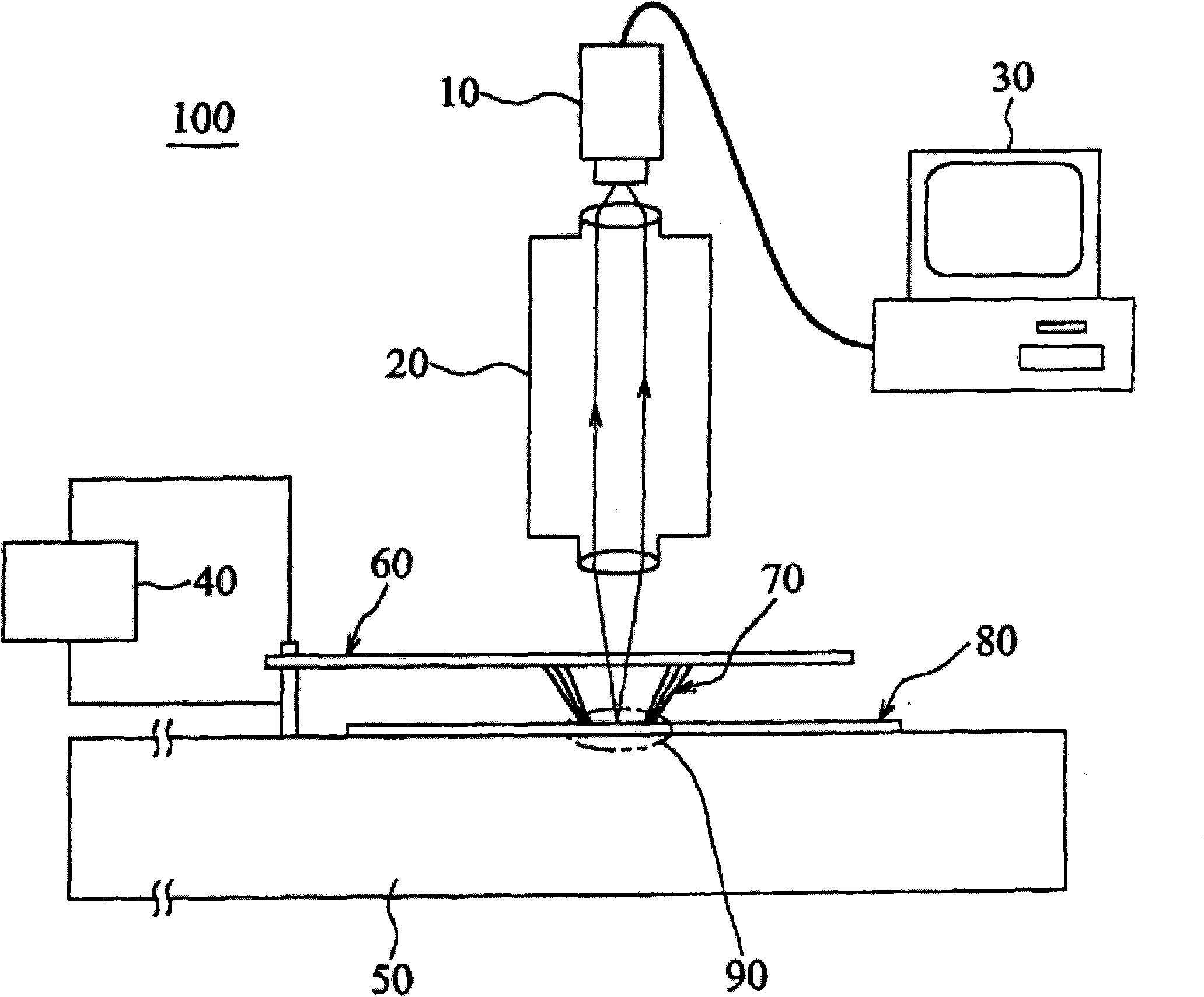
[0015] As mentioned above, the radio frequency power amplifier in the mobile phone is a large-scale transistor cell array configured by dozens of transistors in parallel. These transistors are mainly silicon bipolar transistors, gallium arsenide metal-semiconductor field effect transistors Arsenic heterojunction bipolar transistor, wherein when the gallium arsenic heterojunction bipolar transistor is energized, the base region of the bipolar transistor will undergo radiation recombination, that is, emit infrared light. Therefore, the present invention detects the integrated circuit through the infrared light image display device, so as to search out defective products in the integrated circuit.

[0016] figure 1 In one embodiment of the present invention, it represents the detection device architecture for implementing the method for detecting defective integrated circuits. Such as figure 1 As shown, the detection device 100 that realizes the defective product detection meth...


PUM


Abstract

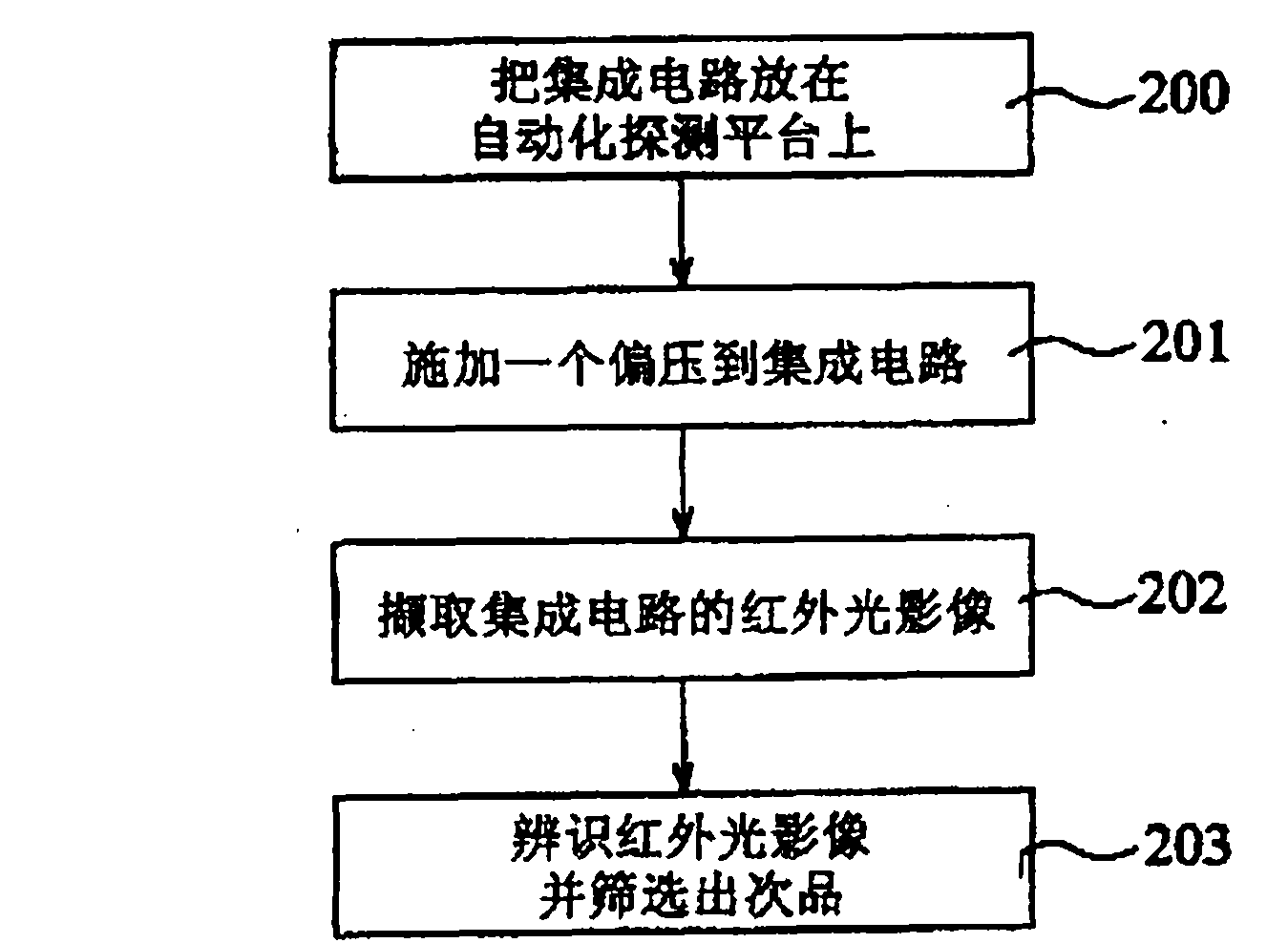
The invention relates to a screening method for an integrated circuit IC. The integrated circuit is formed by connecting a plurality of transistors on a wafer in parallel. The method comprises the following steps: applying bias voltage on the transistors; and capturing infrared light images of the transistors. The screening method disclosed by the invention has the advantages of high detection speed, automation and high detection accuracy.

Description

technical field [0001] The invention relates to a method for screening integrated circuits; in particular, it relates to a method for screening defective products of integrated circuits composed of transistors from the wafer stage and packaging stage in the semiconductor process by using the principle of infrared photothermal induction. Background technique [0002] One of the key electronic components of a handheld phone is the RF power amplifier, which usually consists of dozens of transistors connected in parallel to form a large transistor cell array to boost its output power. Currently, integrated circuits with such large transistor cell arrays are usually tested by means of in-line inspection and DC electronic probe testing during the wafer stage and packaging stage of the semiconductor manufacturing process to find defective products. However, these two methods have the following disadvantages in actual use: as far as online inspection is concerned, since only structu...

Claims


Application Information

Patent Timeline
Patent Type & Authority Applications(China)
IPC IPC(8): H01L21/66G01R31/311
Inventor 柯恩清
Owner 上海允科自动化有限公司
Learn More