Chip LED (light emitting diode) display screen and manufacturing method thereof

A technology for an LED display screen and a manufacturing method, applied in the directions of identification devices, instruments, lighting and heating equipment, etc., can solve the problems of poor anti-static ability, poor consistency, and low protection performance, and achieve stable performance and good display effect. , the effect of low power consumption

Inactive Publication Date: 2011-07-13
李海涛
View PDF13 Cites 18 Cited by
  • Summary
  • Abstract
  • Description
  • Claims
  • Application Information

AI Technical Summary

Problems solved by technology

[0002] The LED display screen is composed of LED dot matrix. Text and pictures are displayed by turning on and off the lamp beads. The content can be replaced at any time. Each part of the component is a display device with a modular structure. The display module is composed of a dot matrix composed of LED lights. Responsible for luminous display, LED display can not only be used indoors, but also can be used in outdoor environments, which has incomparable advantages. The development prospect of LED is currently moving towards higher brightness, higher weather resistance, higher luminous density, The direction of higher luminous uniformity is developing. The LED display module currently on the market is to weld the light-emitting diode on the printed circuit board sprayed with black paint, and then weld the nut post on the other side of the printed circuit board, and install it directly through the nut post. On the display screen structure box, this method has many defects. The consistency of black paint sprayed on the printed circuit board is not good, and the protection performance of this process is not high, and the antistatic ability is poor.

Method used


Image

  • Chip LED (light emitting diode) display screen and manufacturing method thereof
  • Chip LED (light emitting diode) display screen and manufacturing method thereof
  • Chip LED (light emitting diode) display screen and manufacturing method thereof

Examples


Embodiment 1

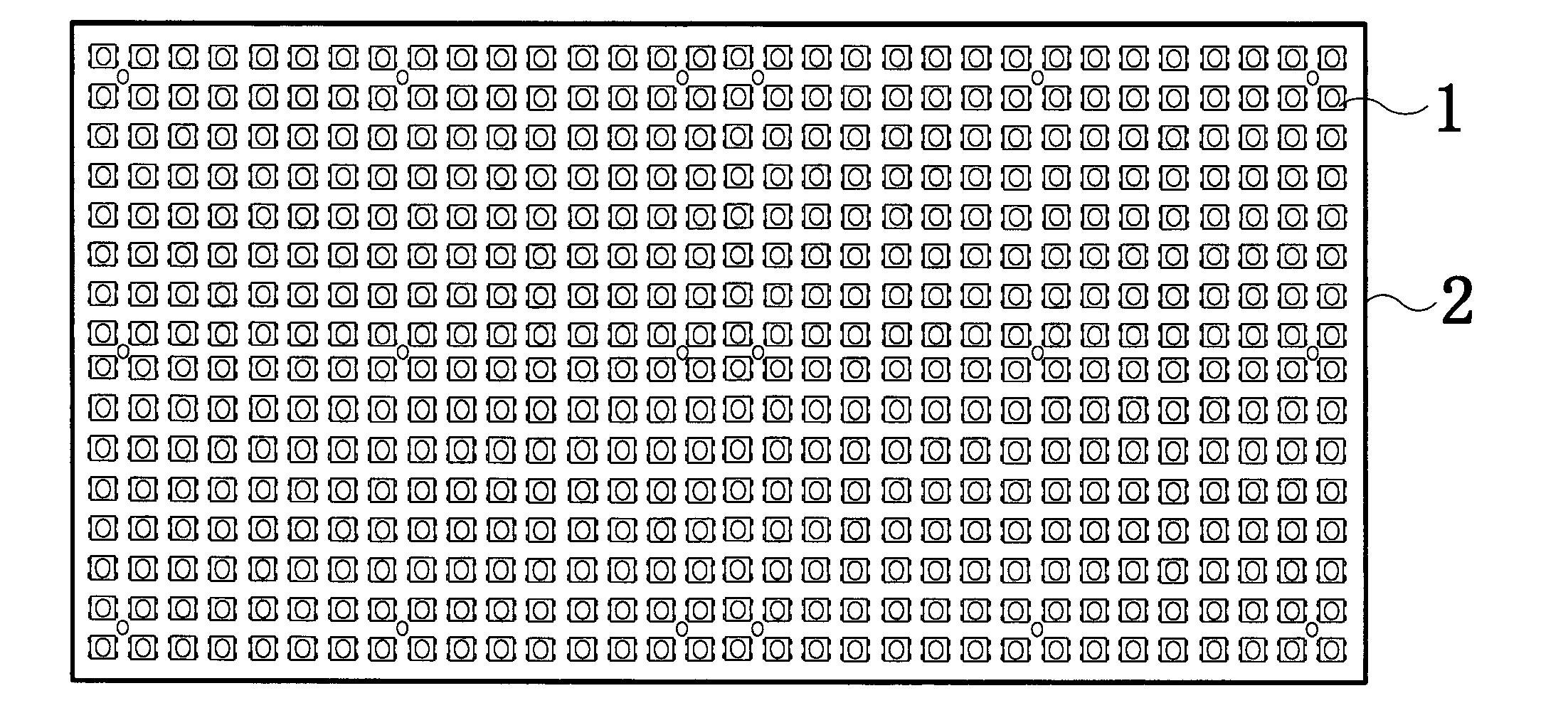
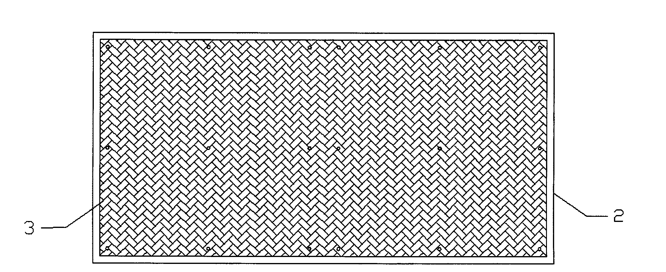
[0039] Step 1. The mounted high-brightness SMD LED lamp 1 is connected to the circuit board 2 by welding, and the reverse side of the circuit board 2 to which the SMD LED lamp 1 is welded is processed with an anti-adhesive protective film 3, see figure 1 and figure 2 ;

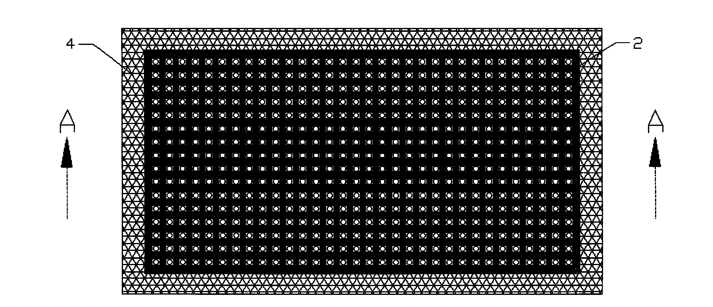
[0040] Step 2. The circuit board 2 and the plastic injection mold 4 after being treated with the anti-adhesive protective film 3 are locked by screws 5, and a black waterproof colloid 7 with a hardness of 60 Shore D is injected into the plastic injection mold through the plastic injection port 6. The liquid level of the waterproof colloid 7 is equal to the height of the top of the SMD LED lamp. The waterproof colloid 7 contains materials that resist ultraviolet rays, acid rain and reduce reflection. After the waterproof colloid 7 is cured, it is demolded and the anti-adhesive protective film 3 is removed. , see image 3 and Figure 4 ;

[0041] Step 3. The excess part of the glue on the edge of the circui...

Embodiment 2

[0045] Step 1. The mounted high-brightness SMD LED lamp 1 is connected to the circuit board 2 by welding, and the reverse side of the circuit board 2 to which the SMD LED lamp 1 is welded is processed with an anti-adhesive protective film 3, see figure 1 and figure 2 ;

[0046] Step 2. The circuit board 2 and the plastic injection mold 4 after being treated by sticking the anti-adhesive protective film 3 are locked by screws 5, and a black waterproof colloid 7 with a hardness of 80 Shore D is injected into the plastic injection mold through the plastic injection port 6. The liquid level of the waterproof colloid 7 is equal to the height of the top of the SMD LED lamp. The waterproof colloid 7 contains materials that resist ultraviolet rays, acid rain and reduce reflection. After the waterproof colloid 7 is cured, it is demolded and the anti-adhesive protective film 3 is removed. , see image 3 and Figure 4 ;

[0047] Step 3. The excess part of the glue on the edge of the...

Embodiment 3

[0051] Step 1. The mounted high-brightness SMD LED lamp 1 is connected to the circuit board 2 by welding, and the reverse side of the circuit board 2 to which the SMD LED lamp 1 is welded is processed with an anti-adhesive protective film 3, see figure 1 and figure 2 ;

[0052] Step 2. The circuit board 2 and the plastic injection mold 4 after being treated with the anti-adhesive protective film 3 are tightened and assembled through the screws 5, and the black waterproof colloid 7 with a hardness of 65 Shore D is injected into the plastic injection mold through the plastic injection port 6. The liquid level of the waterproof colloid 7 is level with the top of the SMD LED lamp. The waterproof colloid completely covers the circuit board. Due to the wall-climbing effect of the liquid, the waterproof colloid also covers the metal conductive pins of the SMD LED lamp 1. At the same time, the LED and the A groove area is formed between the LEDs;

[0053] Step 3. The excess part of t...


PUM


Abstract

The invention relates to a chip LED (light emitting diode) display screen and manufacturing method thereof. The chip LED display screen comprises chip LED lamps, a circuit board, a driving component, a waterproof colloid and a bottom shell, wherein the chip LED lamps are uniformly welded on the circuit board; the driving component is welded on the circuit board; and the circuit board is arranged on the bottom shell. The manufacturing method comprises the following steps of: welding and connecting the chip LED lamps with the circuit board; adhering film at the rear side of the circuit board; fastening the circuit board and a glue injection mold by screw bolts; injecting the waterproof colloid in the glue injection mold; cutting off residual colloid on the edges of the circuit board; cutting shaped lines on the surface of the colloid between the LEDs; welding the driving component at the rear side of the circuit board; locking and assembling the circuit board and the bottom shell by screws; adhering film at the periphery of the contact surface of the bottom shell and the circuit board; and injecting the waterproof colloid in a cavity of the bottom shell. The chip LED display screen provided by the invention is waterproof, moisture-proof, long in service life and uniform in illumination. The manufacturing method in the invention is simple and can be popularized.

Description

technical field [0001] The invention relates to an LED display screen, in particular to a patch LED display screen and a manufacturing method thereof. Background technique [0002] The LED display screen is composed of LED dot matrix. Text and pictures are displayed by the light on and off of the lamp beads. The content can be replaced at any time. Each part of the components is a display device with a modular structure. The display module is composed of a dot matrix composed of LED lights. Responsible for luminous display, LED display can be used not only indoors, but also in outdoor environments, with incomparable advantages. The development prospect of LED is currently moving towards higher brightness, higher weather resistance, higher luminous density, The direction of higher luminous uniformity is developing. At present, the LED display module on the market is to weld the LED on the printed circuit board sprayed with black paint, and then weld the standoff on the other ...

Claims


Application Information

Patent Timeline
Patent Type & Authority Applications(China)
IPC IPC(8): G09F9/33F21V19/00F21V31/04F21Y101/02F21Y105/16F21Y115/10
Inventor 李海涛
Owner 李海涛
Why Eureka
Try Eureka