Method for manufacturing bipolar junction transistor

A technology of bipolar transistor and fabrication method, applied in semiconductor/solid-state device manufacturing, electrical components, circuits, etc., can solve problems such as difficulty in self-alignment with heavy doping, increase in tunnel leakage, etc.

Active Publication Date: 2011-07-13
SHANGHAI HUAHONG GRACE SEMICON MFG CORP
View PDF4 Cites 11 Cited by
  • Summary
  • Abstract
  • Description
  • Claims
  • Application Information

AI Technical Summary

Problems solved by technology

Moreover, the dense doping required by the extrinsic base region in the above process is difficult to easily achieve self-alignment w...

Method used


Image

  • Method for manufacturing bipolar junction transistor
  • Method for manufacturing bipolar junction transistor
  • Method for manufacturing bipolar junction transistor

Examples


Embodiment Construction

[0017] In order to make the content of the present invention clearer and easier to understand, the content of the present invention will be further described below in conjunction with the accompanying drawings. Of course, the present invention is not limited to this specific embodiment, and general replacements known to those skilled in the art are also covered within the protection scope of the present invention.

[0018] Secondly, the present invention is described in detail by means of schematic diagrams. When describing the examples of the present invention in detail, for the convenience of explanation, the schematic diagrams are not partially enlarged according to the general scale, which should not be used as a limitation of the present invention.
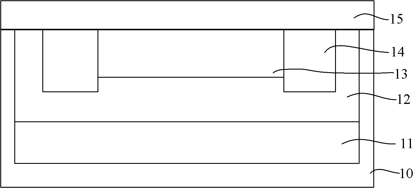
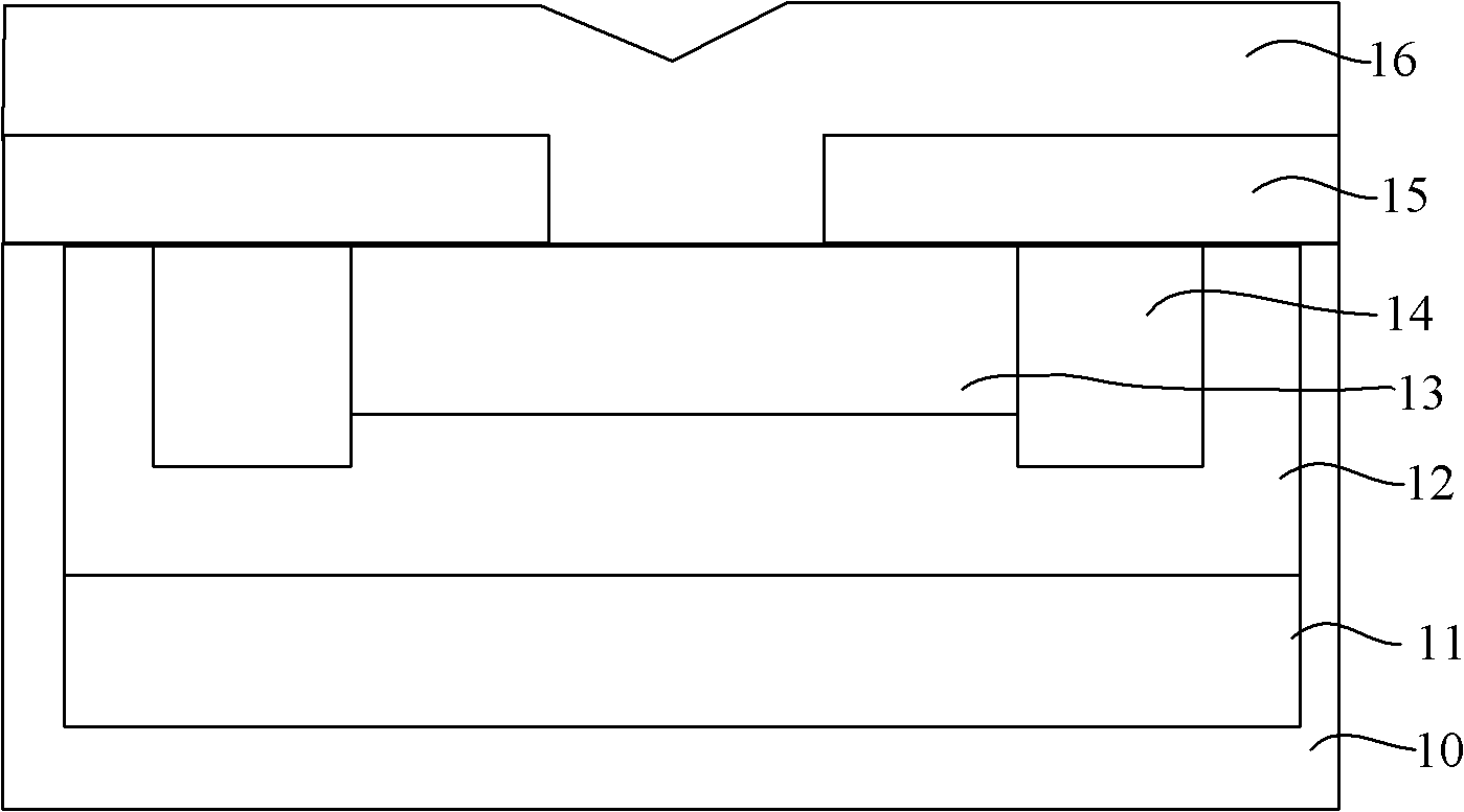
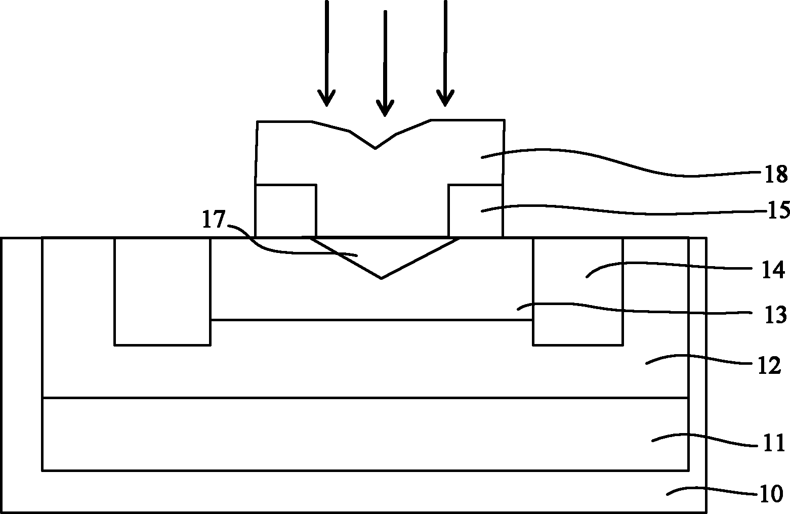
[0019] The core idea of ​​the present invention is: at the same time as the formation process of the CMOS transistor, the oxidation of the polysilicon emitter and the emitter of the bipolar transistor is formed synchronously b...


PUM


Abstract

The invention relates to a method for manufacturing a bipolar junction transistor, which is compatible with a process for preparing a complementary metal oxide semiconductor (CMOS) transistor. In the method, an emitter is formed in a bipolar junction transistor preparation region while gate polycrystalline silicon is formed in a CMOS transistor preparation region; high doping is generally required to be performed on an extrinsic base region in the bipolar junction transistor so as to form good ohmic contact with an electrode; a self-aligned extrinsic base region is realized by means of self-aligned high-doping ion implantation of the CMOS transistor; and doping ions are implanted and propelled to the emitter, so that the doping ions are uniformly propelled to the base region to form an emitter junction, the thickness of the emitter junction is more uniform, and etching damage is repaired by means of a rapid thermal oxidation process of a CMOS polycrystalline silicon gate after a polycrystalline silicon layer is etched; therefore, the boundary effect is reduced and the leakage current is reduced.

Description

technical field [0001] The invention relates to a semiconductor manufacturing process, in particular to a manufacturing method of a bipolar transistor compatible with a CMOS transistor manufacturing process. Background technique [0002] Bipolar Junction Transistor (BJT) is one of the common device structures constituting modern large-scale integrated circuits. It has fast operation speed, small saturation voltage drop, high current density and low production cost. A bipolar transistor is an electronic component that uses two types of carriers (Carries), electrons and holes (holes), to conduct current. The structure of a bipolar transistor is a three-terminal ( Three Terminal) components. The three terminals are Emitter, Base and Collector. [0003] Figure 1a ~ Figure 1c It is a structural schematic diagram of the formation process of the bipolar transistor in the prior art, such as Figure 1a ~ Figure 1c As shown, the step of forming a bipolar transistor in the prior art...

Claims


Application Information

Patent Timeline
IPC IPC(8): H01L21/8249H01L21/331
Inventor 吴小利
Owner SHANGHAI HUAHONG GRACE SEMICON MFG CORP
Why Eureka
Try Eureka