Method for filling redundancy metal

A technology of redundant metal and metal wires, applied in the fields of instruments, computing, electrical and digital data processing, etc., can solve the problems of reduced circuit layout flatness, large capacitance increment, etc., to ensure consistency, improve yield, and prevent damage Effect

Active Publication Date: 2011-07-20
INST OF MICROELECTRONICS CHINESE ACAD OF SCI
View PDF3 Cites 16 Cited by
  • Summary
  • Abstract
  • Description
  • Claims
  • Application Information

AI Technical Summary

Problems solved by technology

[0008] The purpose of the present invention is to at least solve one of the above-mentioned technical problems, especially solve the problem that the flatness of the circuit layout after wiring is reduced and the capacitance increase between lines is too large after adding redundant metal

Method used


Image

  • Method for filling redundancy metal
  • Method for filling redundancy metal
  • Method for filling redundancy metal

Examples


Embodiment Construction

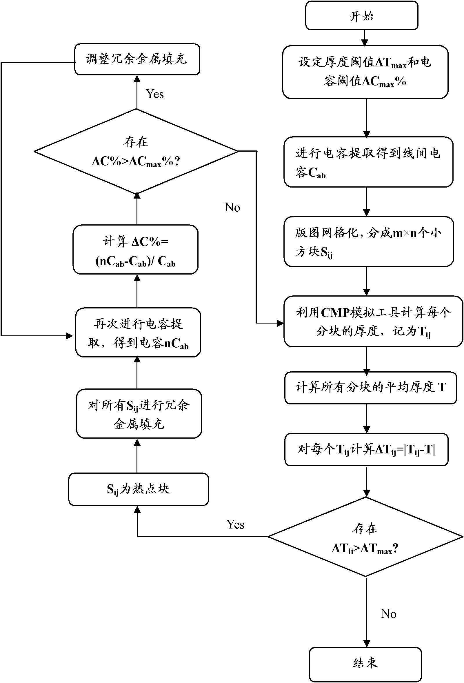
[0032] Embodiments of the present invention are described in detail below, examples of which are shown in the drawings, wherein the same or similar reference numerals designate the same or similar elements or elements having the same or similar functions throughout. The embodiments described below by referring to the figures are exemplary only for explaining the present invention and should not be construed as limiting the present invention.

[0033] The following disclosure provides many different embodiments or examples for implementing different structures of the present invention. To simplify the disclosure of the present invention, components and arrangements of specific examples are described below. Of course, they are only examples and are not intended to limit the invention. Furthermore, the present invention may repeat reference numerals and / or letters in different instances. This repetition is for the purpose of simplicity and clarity and does not in itself indicat...


PUM


Abstract

The invention discloses a method for filling a redundancy metal in a semiconductor manufacturing process. In the method, redundancy metal filling is evaluated and adjusted by combining analogue flatness and extracting the capacitance between metal wires; and all flatness hotspots and capacitance hotspots of a circuit layout are eliminated by a plurality of iteration processes; therefore, not onlythe consistency of the circuit layout thickness after performing chemical mechanical polishing (CMP) can be ensured to improve the yield of chips, but also the damage to functions of the chips causedby the introduction of the redundancy metal can be prevented to ensure the signal completeness of the metal wires in the circuit layout.

Description

technical field [0001] The invention relates to the technical field of circuit manufacturing technology and layout design, in particular to a method for filling redundant metal according to chip surface thickness and metal line coupling capacitance. Background technique [0002] In the manufacturing process of an integrated circuit (IC), various methods such as physical vapor deposition and chemical vapor deposition are usually used to deposit metals, dielectrics and other materials on the surface of a silicon wafer to form a multilayer metal structure. In the manufacture of each layer of the metal structure, it is necessary to ensure that the surface of the metal layer has better flatness. If the flatness of the surface is not good, it will affect the depth of focus level required in lithography, thereby reducing the yield. A circuit with better flatness can ensure that the metal structure is not easily deformed throughout the forming process. [0003] In order to obtain ...

Claims


Application Information

Patent Timeline
Patent Type & Authority Applications(China)
IPC IPC(8): H01L21/768H01L21/82G06F17/50
Inventor 马天宇陈岚阮文彪李志刚叶甜春
Owner INST OF MICROELECTRONICS CHINESE ACAD OF SCI
Why Eureka
Try Eureka