P-channel depletion MOS (metal oxide semiconductor) transistor and preparation method thereof

A MOS transistor and depletion-type technology, which is applied in the field of P-channel depletion-type MOS transistors and its preparation, can solve the problems of increased production costs, complicated manufacturing processes, and waste of resources.

Inactive Publication Date: 2011-07-27
PEKING UNIV FOUNDER GRP CO LTD +1
View PDF4 Cites 16 Cited by
  • Summary
  • Abstract
  • Description
  • Claims
  • Application Information

AI Technical Summary

Problems solved by technology

Its production process is complex, requiring multiple photolithography and ion implantation (the whole process incl

Method used


Image

  • P-channel depletion MOS (metal oxide semiconductor) transistor and preparation method thereof
  • P-channel depletion MOS (metal oxide semiconductor) transistor and preparation method thereof
  • P-channel depletion MOS (metal oxide semiconductor) transistor and preparation method thereof

Examples


Embodiment Construction

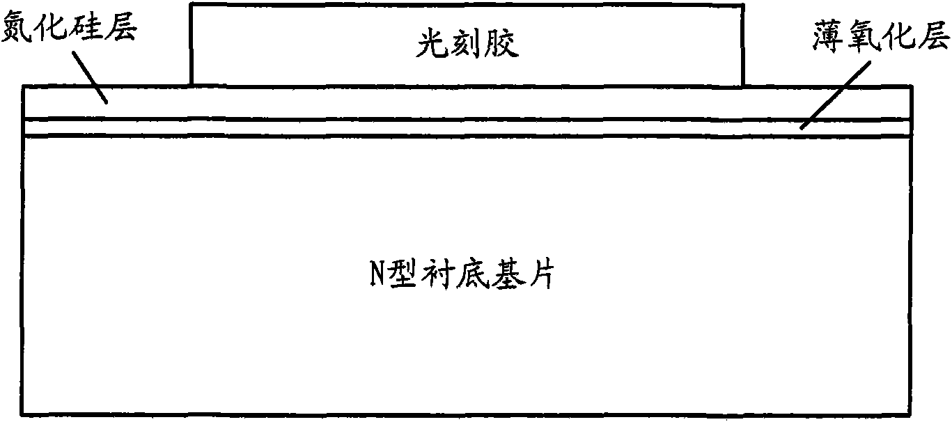
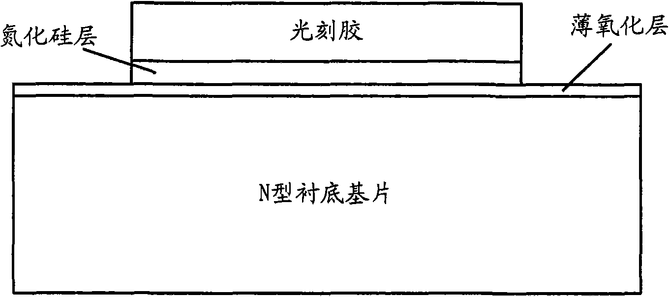
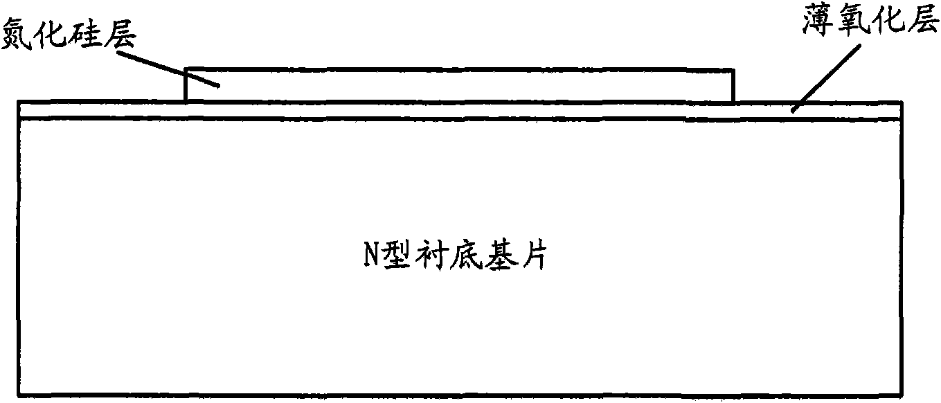
[0097] The preparation method of the P channel depletion mode MOS transistor provided by the embodiment of the present invention, its process is as follows Figure 14 As shown, it mainly includes the following process steps:

[0098] Step S11: preparing a field oxide layer on the upper surface of the N-type substrate outside the region where the MOS electrodes are to be prepared.

[0099] Step S12: preparing a gate oxide layer in the area not covered by the field oxide layer.

[0100] Step S13 : preparing an undoped polysilicon layer in the area where the MOS gate is to be prepared on the gate oxide layer.

[0101] Step S14: implant a set dose of boron ions from the area above the N-type substrate that is not covered by the field oxide layer, so that the undoped polysilicon layer forms a P-type polysilicon layer, and the undoped polysilicon layer A P-type source (drain) region is formed with the surface layer region above the N-type substrate covered by the field oxide layer...


PUM

PropertyMeasurementUnit
Thicknessaaaaaaaaaa
Thicknessaaaaaaaaaa
Thicknessaaaaaaaaaa

Abstract

The invention discloses a P-channel depletion MOS (metal oxide semiconductor) transistor and a preparation method thereof. The method comprises the following steps: preparing a field oxide layer on the upper surface outside an area of an MOS electrode to be prepared of an N-type substrate, and preparing a gate oxide layer on an area which is not covered by the field oxide layer; preparing an undoped polysilicon layer on an area of an MOS gate to be prepared on the gate oxide layer; injecting boron ions of the set dosage into the area which is not covered by the field oxide layer above the N-type substrate so that the undoped polysilicon layer forms a P-type polysilicon layer and the surface layer on the N-type substrate which is not covered by the undoped polysilicon layer and the field oxide layer forms a P-type source (drain) area; and performing annealing treatment on the N-type substrate after the source (drain) area and the P-type polysilicon layer are formed so as to obtain the P-channel depletion MOS transistor. The method simplifies the preparation process and increases the start voltage of the transistor.

Description

technical field [0001] The invention relates to the technical field of semiconductors, in particular to a P-channel depletion MOS (Metal-Oxide-Semiconductor, Metal-Oxide-Semiconductor) transistor and a preparation method thereof. Background technique [0002] The turn-on voltage of the P-channel enhancement MOS transistor is less than 0, and the transistor is turned on only when the voltage value is less than the turn-on voltage. Therefore, when the difference between the gate and source voltage of the P-channel enhancement MOS transistor (referred to as "gate-source When the voltage ") is 0, the MOS tube cannot be turned on; the turn-on voltage of the P-channel depletion MOS transistor is greater than 0, therefore, when the gate-source voltage is 0, the MOS tube can be turned on, that is, between the source and the drain conduction between. [0003] In the traditional P-channel depletion-mode MOS transistor manufacturing process, a P-type conductive channel is generally fa...

Claims


Application Information

Patent Timeline
IPC IPC(8): H01L21/336H01L29/78H01L21/265H01L29/10
Inventor 潘光燃马万里张立荣
Owner PEKING UNIV FOUNDER GRP CO LTD
Why Eureka
Try Eureka