
Application method of object manufacture defect

An application method and defect technology, applied in the application field of object manufacturing defects, can solve problems such as misjudgment, and achieve the effect of accurate misjudgment and accurate estimation

Active Publication Date: 2013-07-17
吕一云
View PDF1 Cites 0 Cited by
  • Summary
  • Abstract
  • Description
  • Claims
  • Application Information

AI Technical Summary

Problems solved by technology

This can lead to wrong judgments

Method used


Image

  • Application method of object manufacture defect
  • Application method of object manufacture defect
  • Application method of object manufacture defect

Examples


no. 1 example

[0065] Besides the first embodiment, the method further has a second preferred embodiment. The second embodiment also takes a wafer as an example of an item, and can be implemented in the design company 10 or the manufacturing plant 20 .

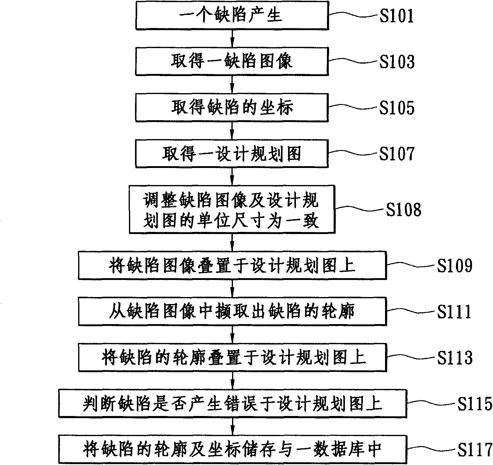
[0066] Please refer to Figure 11 shown, and with reference figure 2 , image 3 and Figure 4 , the detailed flow of the second embodiment of the method is proposed as follows, which is similar to the flow of the first embodiment. That is to say, steps S401 to S407 are the same as steps S101 to S107, and steps S415 to S417 are respectively the same as steps S115 to S117, so the following description will focus on steps S409 and S413.

[0067] In step S409 , the defect image 100 will eventually be superimposed on the design plan 200 according to the coordinates of the defect 101 , but it is completed in two detailed steps. Please refer to Figure 12 As shown, first, according to the coordinates of the defect 101, a partial design plan ...


PUM


Abstract

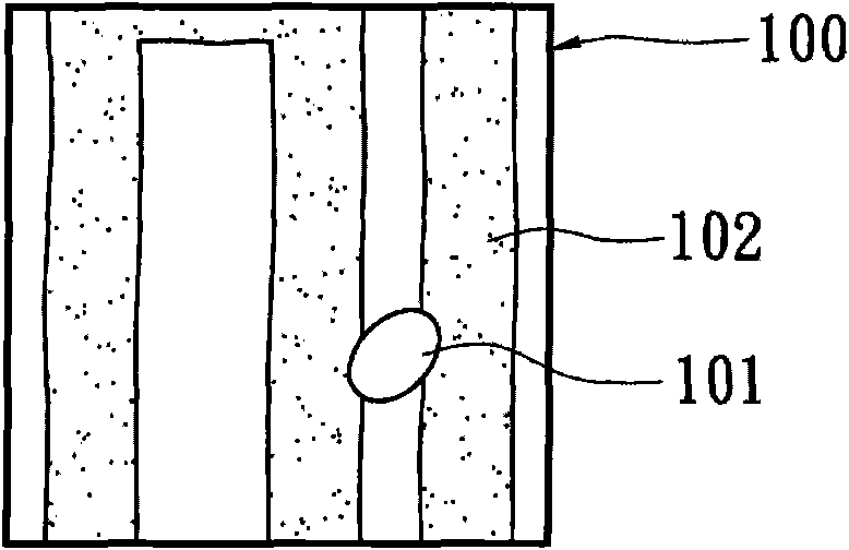
The invention discloses an application method of object manufacture defects, comprising the following steps: obtaining a defect image in the object manufacturing process, wherein the defect image comprises a defect and a plurality of manufactured circuit patterns around the defect; obtaining the coordinate of the defect; obtaining a design planning drawing of the object, wherein the design planning drawing comprises a plurality of design circuit patterns; regulating the unit size of the defect image and the unit size of the design planning drawing to be consistent; capturing the outline of the defect from the defect image; according to the coordinate of the defect, setting the outline of the defect on the design planning drawing; and according to the overlapping situation of the outline of the defect and the design circuit patterns, judging whether the defect causes an open circuit fault or a short circuit fault on the design planning drawing or not. Thus, the health condition of the object can be monitored in the manufacture process and can be known before the manufacture process ends.

Description

technical field [0001] The invention relates to a method for applying manufacturing defects of articles. Background technique [0002] The manufacturing methods of integrated circuit dies include thin film deposition, mask alignment, photolithography and etching. In these manufacturing processes, every process and equipment will cause defects every day, which will affect the pass rate of products. The pass rate of the product is directly related to the cost of the chip. [0003] However, IC design houses do not have relevant knowledge or know how to control the yield of their products in the manufacturing stage. So the design house will not know about the occurrence of low-yield errors until the design house receives and tests the wafers from the foundry fab. If the pass rate of wafers or packaged products is lower than the demand, the design company will face the problem of not being able to ship to customers and poor quality. It took months to make up the shortfall to ...

Claims


Application Information

Patent Timeline
Patent Type & Authority Patents(China)
IPC IPC(8): H01L21/00H01L21/66G01R31/02G01N21/88
Inventor 吕一云
Owner 吕一云
Learn More