Integrated magnetic electronic signal isolation coupling device and preparation process of integrated magnetic electronic signal isolation coupling device

An electronic signal, isolation coupling technology, applied in the field of integrated magnetoelectronic signal isolation coupling device and its preparation process, can solve the problems of uncertain output signal state, limited flip speed, difficult integration, etc., and achieve reasonable preparation process steps and signal isolation Interference, the effect of easy industrial production

Active Publication Date: 2011-08-10
武汉嘉晨电子技术有限公司
View PDF2 Cites 2 Cited by
  • Summary
  • Abstract
  • Description
  • Claims
  • Application Information

AI Technical Summary

Problems solved by technology

Optocouplers have the following essential disadvantages: large size, slow speed (<10 MHz), difficult integration, no radiation protection and easy aging
However, there are three main disadvantages of this giant magnetoresistance (GMR) magnetoelectric coupling device: the first is that the device is not fully compatible with the optocoupler, and a dedicated driver is needed to convert the voltage signal into a current signal; After a power loss, the state of the output signal is indeterminate after a restart
The third is that the magnetization switching of the free layer involves domain wall motion, which not only produces Barkhausen noise, but also limits the switching speed

Method used


Image

  • Integrated magnetic electronic signal isolation coupling device and preparation process of integrated magnetic electronic signal isolation coupling device
  • Integrated magnetic electronic signal isolation coupling device and preparation process of integrated magnetic electronic signal isolation coupling device
  • Integrated magnetic electronic signal isolation coupling device and preparation process of integrated magnetic electronic signal isolation coupling device

Examples


Embodiment

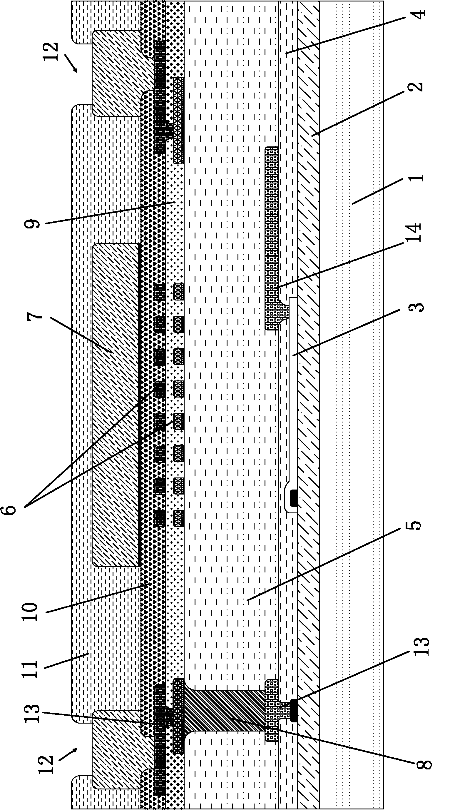
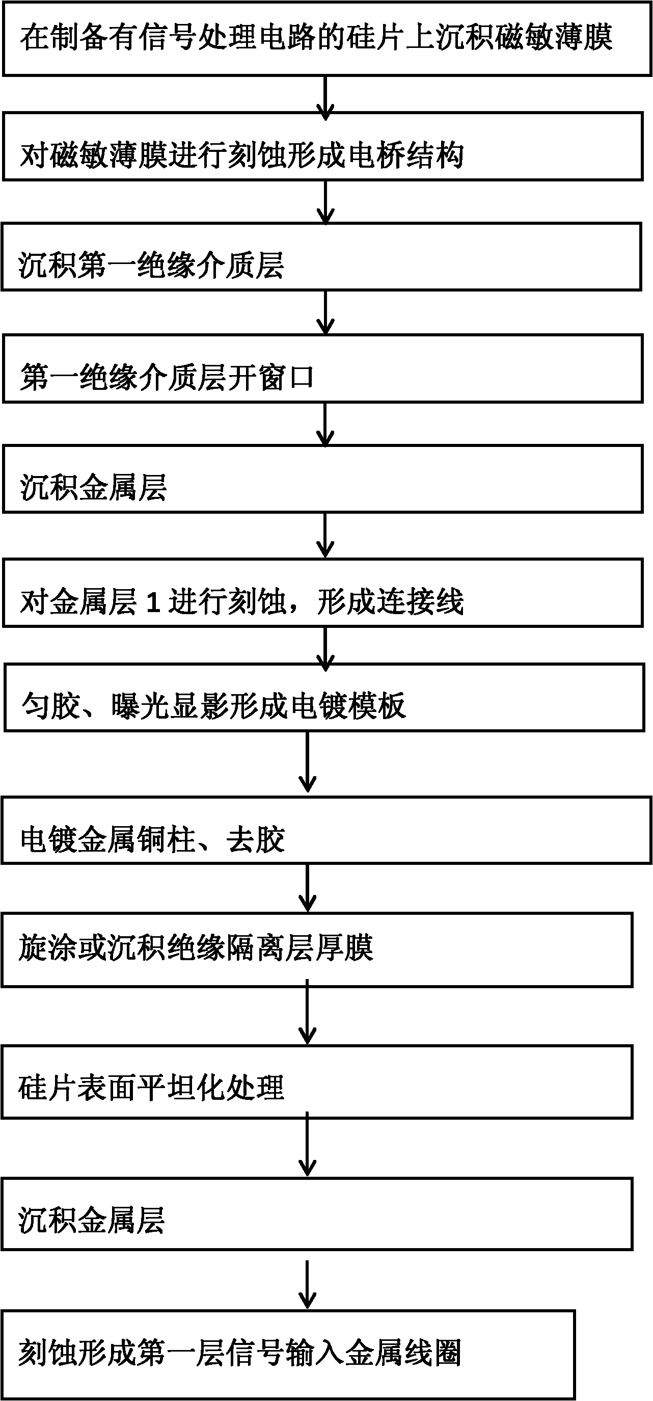
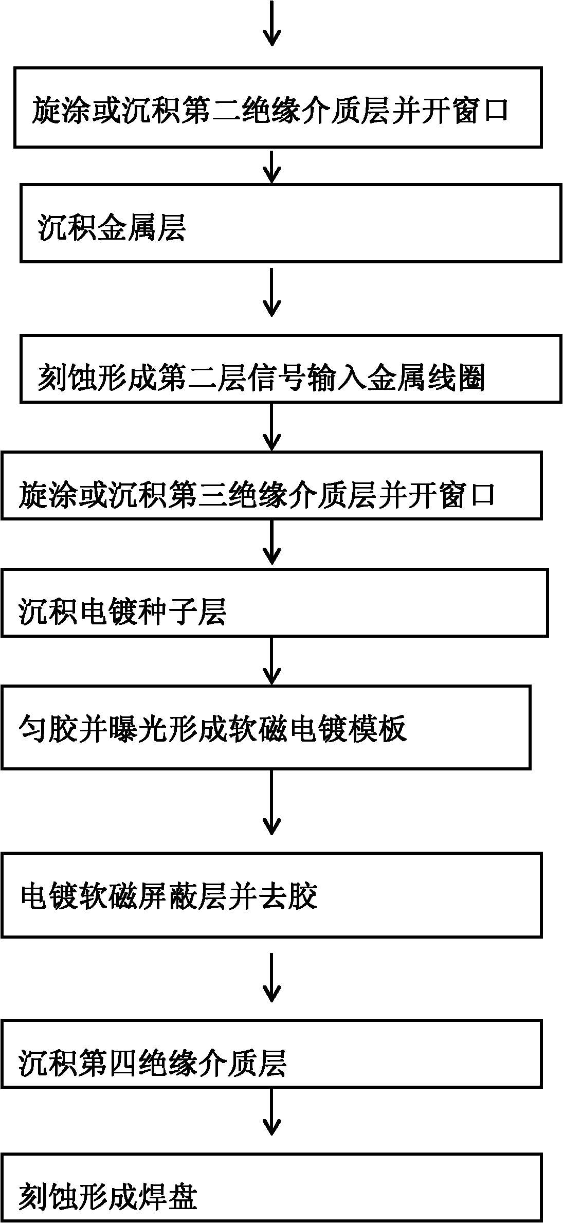
[0023] Example: Integrated magnetic and electronic signal isolation coupling devices, such as figure 1 As shown, it includes a signal input coil 6 , a magnetic sensitive bridge 3 connected to the signal input coil 6 , and a signal processing circuit 2 connected to the magnetic sensitive bridge 3 . The above three are integrated on the same die, from bottom to top: signal processing circuit 2, first insulating medium layer 4, magnetic sensitive bridge 3, insulating isolation layer 5, signal input coil 6, soft magnetic shielding layer 7 , the magnetic sensitive bridge 3 and the signal processing circuit 2 are completely isolated electrically from the signal input coil. The magneto-sensitive bridge 3 includes a linear giant magnetoresistance, that is, a GMR magneto-sensing unit, or a magnetic tunnel junction, that is, an MTJ magneto-sensing unit. The magneto-sensitive bridge 3 , the power supply end and the signal output end of the signal processing circuit 2 are respectively ...


PUM


Abstract

The invention relates to an integrated magnetic electronic signal isolation coupling device and a preparation process of the integrated magnetic electronic signal isolation coupling device. The coupling device sequentially comprises a signal processing circuit, a first insulated dielectric layer, a magnetic sensitive bridge, an insulated isolating layer, a signal input coil and a soft magnetic shielding layer from bottom to top, wherein the magnetic sensitive bridge and the signal processing circuit are electrically completely isolated from the signal input coil. The preparation process comprises the steps of preparing the magnetic sensitive bridge; preparing the insulated isolating layer and an opening; depositing a metal layer and etching to form a connecting line; taking photoresist asa template to form a copper column through a plating process; preparing the signal input coil; and adding the soft magnetic shielding layer on the signal input coil and depositing the insulated isolating layer. The coupling device has the remarkable and substantial characteristics that the coupling device is provided with the signal input coil with a double-layer structure, and an input signal current welding plate is arranged outside the coil, therefore, the overall layout of a chip is convenient, the size of the chip is reduced, and the unit current can generate strong magnetic signals whenpassing through the double-layer coil.

Description

Technical field [0001] The invention relates to an integrated magnetoelectronic signal isolation coupling device and a preparation process thereof. Background technique [0002] Isolated signal coupling devices are widely used in computer network interfaces, data transmission, communications, sensors / measuring instruments, mobile electronics, medical electronics and other fields. The basic function of the isolation signal coupling device is to communicate data signals in a state of electrical isolation. Isolation signal coupling devices can reduce or eliminate ground loop noise and common mode voltage effects and the resulting damage to the interface and auxiliary circuits. Now widely used is the photoelectric signal isolation coupling device (hereinafter referred to as photocoupler), whose operating principle is based on the emission and detection of optical signals. The optocoupler is composed of an optical signal transmitter and a detector separated by an optically tran...

Claims


Application Information

Patent Timeline
Patent Type & Authority Applications(China)
IPC IPC(8): H01L43/00H01L43/12
Inventor 钱正洪
Owner 武汉嘉晨电子技术有限公司
Why Eureka
Try Eureka