Device and method for detecting alignment parameter of photoetching machine

The technology of a detection device and detection method is applied in the direction of the photoplate making process of originals, optics, and patterned surfaces for photomechanical processing, and can solve the problems of complex detection methods and low production efficiency.

Inactive Publication Date: 2011-08-17
SEMICON MFG INT (SHANGHAI) CORP
View PDF2 Cites 39 Cited by
  • Summary
  • Abstract
  • Description
  • Claims
  • Application Information

AI Technical Summary

Problems solved by technology

[0007] In order to solve the problems of the existing lithography machine alignment parameter detection device and its detection method being complex and low production efficiency, it is necessary to provide a simple and high production efficiency lithography machine alignment parameter detection device

Method used


Image

  • Device and method for detecting alignment parameter of photoetching machine
  • Device and method for detecting alignment parameter of photoetching machine
  • Device and method for detecting alignment parameter of photoetching machine

Examples


Embodiment Construction

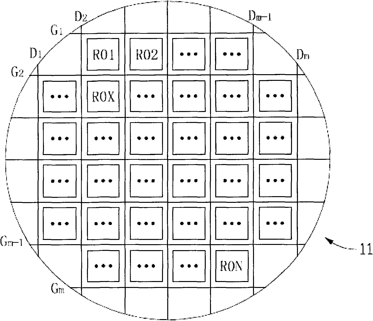
[0032] The device for detecting the alignment parameters of the photolithography machine and the detection method thereof according to the present invention will be described in detail below in conjunction with the accompanying drawings. Before describing the detection device for the alignment parameters of the lithography machine of the present invention, the structure of the wafer used as the basis for producing integrated circuit chips in this embodiment will be described first.

[0033] see figure 1 , which is a schematic diagram of the structure of the wafer of the present invention. The wafer 11 includes m first dicing lines G1, G2, . Tracks D1 , D2 , . . . , Dm-1 , Dm and a plurality of exposure regions R01 , R02 , . . . , R0X, . The multiple first cutting lines G1, G2, . . . , Gm-1, Gm are perpendicular to the multiple second cutting lines D1, D2, ..., Dm-1, Dm. Every two adjacent first scribe lines Gm and every two adjacent second scribe lines Dm correspond to defi...


PUM


Abstract

The invention provides a device and a method for detecting an alignment parameter of a photoetching machine, and relates to the field of semiconductor manufacture technologies. The detection device comprises a mask plate; the mask plate comprises a first alignment mark and a second alignment mark to determine the alignment parameter of the photoetching machine by matching a wafer; the wafer comprises a plurality of first cutting paths and a plurality of second cutting paths; the first cutting paths are parallel with one another and extend along a horizontal direction, and the second cutting paths are parallel with one another and vertical to the first cutting paths; the plurality of first cutting paths and the plurality of second cutting paths define a plurality of exposure regions; the first alignment mark and the second alignment mark are identical in shape and different in size; and after a wafer patterning technology, a wafer mark pattern laminated by the first alignment mark and the second alignment mark is formed between two adjacent exposure regions. The detection method and the detection device are simple, and high in production efficiency.

Description

technical field [0001] The invention relates to a detection device and a detection method of a semiconductor manufacturing process, in particular to a detection device and a detection method of alignment parameters of a photolithography machine. Background technique [0002] With the development of semiconductor technology, the area of ​​semiconductor chips is getting smaller and smaller, and the critical dimensions of semiconductor devices in the chip are also shrinking, so the requirements for semiconductor technology precision are getting higher and higher. In the manufacturing process of semiconductor devices, more than 20 layers of different mask patterns need to be superimposed on the wafer in sequence. In order to ensure the conductivity of semiconductor devices, each layer pattern needs to have a good overlay with other layer patterns precision. [0003] In order to transfer the mask pattern to the wafer correctly, the key step is to align the mask with the wafer. I...

Claims


Application Information

Patent Timeline
Patent Type & Authority Applications(China)
IPC IPC(8): G03F9/00G03F1/14
Inventor 夏婷婷
Owner SEMICON MFG INT (SHANGHAI) CORP
Why Eureka
Try Eureka