Method for reducing surface light reflectivity of silicon chip

A technology of light reflectivity and silicon wafer surface, applied in the direction of sustainable manufacturing/processing, electrical components, climate sustainability, etc., can solve the problems of complex process and high cost, achieve low light reflectivity, low cost, and benefit The effect of large-scale industrial production

Inactive Publication Date: 2011-08-17
INST OF PHYSICS - CHINESE ACAD OF SCI
View PDF5 Cites 32 Cited by
  • Summary
  • Abstract
  • Description
  • Claims
  • Application Information

AI Technical Summary

Problems solved by technology

[0011] The purpose of the present invention is to provide a method for reducing the light reflectivity of the silicon wafer surface, so as to solve the defects of complex process and high cost of the prior art method

Method used


Image

  • Method for reducing surface light reflectivity of silicon chip
  • Method for reducing surface light reflectivity of silicon chip
  • Method for reducing surface light reflectivity of silicon chip

Examples


Embodiment 1

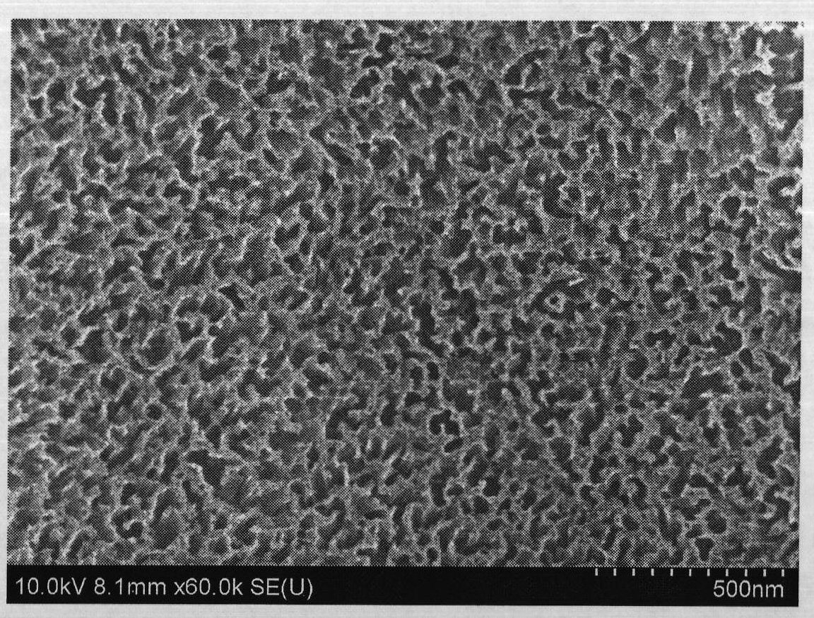
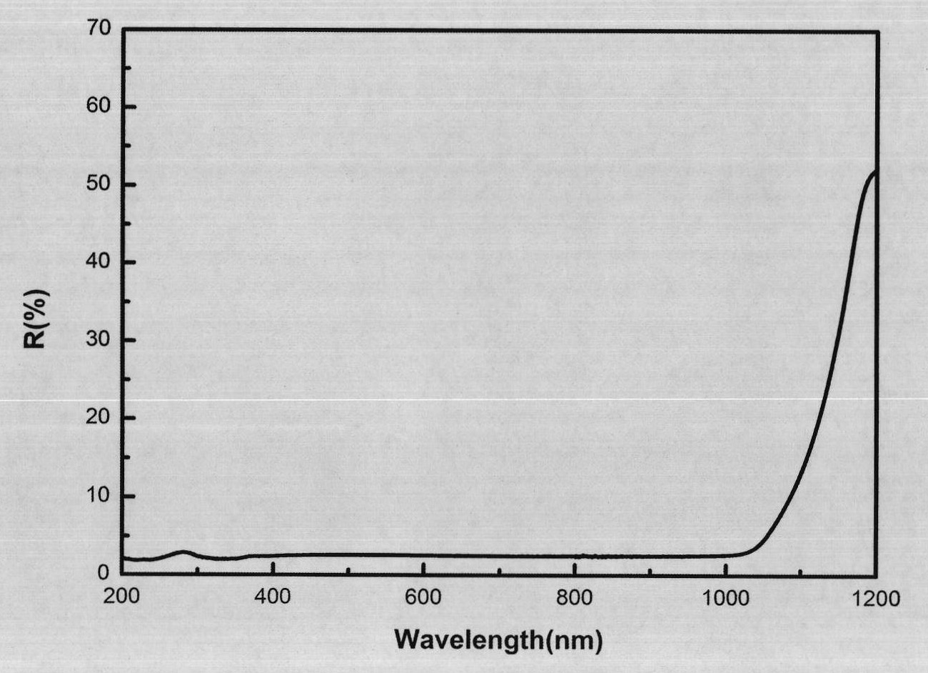
[0051] Clean the p-type Si(100) with a size of 125mm×125mm (resistivity 1-3Ωcm) by traditional techniques, and immerse the silicon wafer in a mixed solution containing 5.1mol / L hydrofluoric acid and 0.03mol / L silver nitrate , etch for 3 min. Then the silicon wafer was taken out, ultrasonically cleaned with nitric acid (concentration 68%) to remove the metal covered on the surface, then ultrasonically cleaned with deionized water, and then dried with high-purity nitrogen to obtain black silicon with low reflectivity. SEM of the light-trapping structure on the silicon surface after etching figure 1 As shown, a nanoporous structure is formed on the surface of the silicon wafer. The obtained reflectance is as figure 2 shown.

Embodiment 2

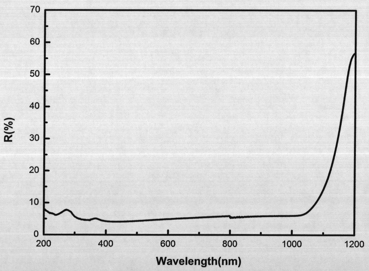
[0053] Clean the p-type Si(100) with a size of 125mm×125mm (resistivity 1~3Ωcm) with traditional technology, and immerse the silicon wafer in a mixed solution containing 5.1mol / L hydrofluoric acid and 0.03mol / L silver nitrate , etch for 4min. Then the silicon wafer is taken out, ultrasonically cleaned with nitric acid to remove the metal covered on the surface, then ultrasonically cleaned with deionized water, and then dried with high-purity nitrogen to obtain black silicon with low reflectivity. The obtained reflectance is as image 3 shown.

Embodiment 3

[0055] Clean the p-type Si(100) with a size of 125mm×125mm (resistivity 1-3Ωcm) by traditional techniques, and immerse the silicon wafer in a mixed solution containing 5.1mol / L hydrofluoric acid and 0.03mol / L silver nitrate , etch for 5min. Then the silicon wafer is taken out, ultrasonically cleaned with nitric acid to remove the metal covered on the surface, then ultrasonically cleaned with deionized water, and then dried with high-purity nitrogen to obtain black silicon with low reflectivity.


PUM


Abstract

The invention discloses a method for reducing the surface light reflectivity of a silicon chip, and the method comprises the following steps: step 1): immerging the silicon chip into mixed solution of hydrofluoric acid and salts containing Ag ions, Cu ions, Ni ions or Mg ions for etching; and step 2): placing the silicon chip after etching into nitric acid or aqua regia for ultrasonic cleaning so as to remove a metal covering object on the surface. The method is simple in process, low in cost, convenient to operate and extensive in application conditions, the complex process is not required, the average light reflectivity of the silicon chip can be reduced to below 5% through only one step, and the method is suitable for large-scale industrial production.

Description

technical field [0001] The invention relates to a method for reducing the surface reflectivity of a silicon wafer. Background technique [0002] With the advancement of science and technology, more and more materials are now used to prepare solar cells. However, due to the good characteristics of silicon itself and its abundant reserves on the earth, silicon-based solar cells are still an important choice in the field of clean energy now and in the future. leading. Since the general silicon surface has a high reflection of sunlight, in order to further improve the conversion efficiency of silicon-based solar cells, the silicon surface must be treated to form various surface light-trapping structures, thereby reducing its reflection of sunlight. [0003] The usual method now is to first etch the silicon surface with acid or alkali to form a pyramid structure, and then coat the surface with an anti-reflective coating (ARCs), such as SiO X ,TiO X , ZnO, SiN X , ITO, etc. H...

Claims


Application Information

Patent Timeline
Patent Type & Authority Applications(China)
IPC IPC(8): H01L31/18
CPCH01L31/02363Y02P70/50
Inventor 刘尧平王燕梅增霞杜小龙
Owner INST OF PHYSICS - CHINESE ACAD OF SCI
Why Eureka
Try Eureka