Antireflective film formation method, antireflective film, and film formation device

A technology of anti-reflection film and film forming method, which is applied in sputtering plating, ion implantation plating, coating, etc., and can solve problems such as inability to form a film

Inactive Publication Date: 2011-08-17
ULVAC INC
View PDF6 Cites 4 Cited by
  • Summary
  • Abstract
  • Description
  • Claims
  • Application Information

AI Technical Summary

Problems solved by technology

[0011] On the other hand, while introducing a reactive gas such as oxygen, when sputtering a Ti target and a Si target to form a film, a large amount of oxygen needs to be introduced, so there is an atmosphere similar to that used to form a transparent conductive film made of metal oxide. The problem of not being able to form a film

Method used


Image

  • Antireflective film formation method, antireflective film, and film formation device
  • Antireflective film formation method, antireflective film, and film formation device
  • Antireflective film formation method, antireflective film, and film formation device

Examples


no. 1 approach

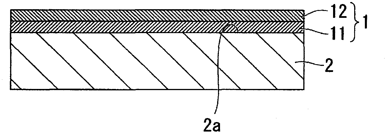
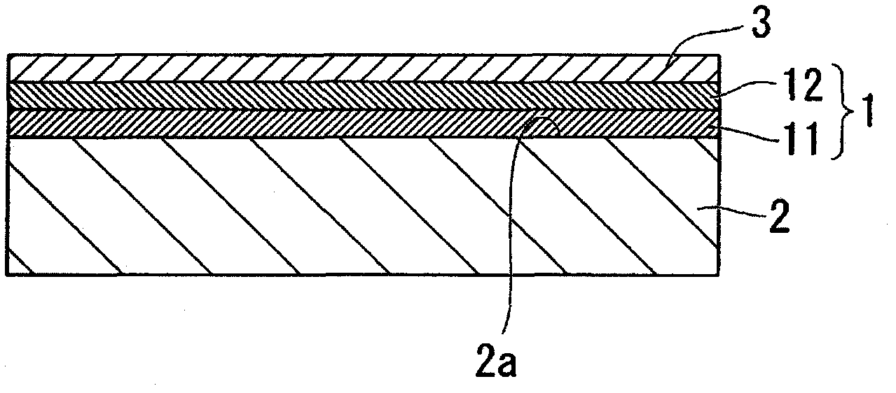
[0048] figure 1 It is a cross-sectional view showing the antireflection film according to the first embodiment of the present invention. The antireflection film 1 is formed on the surface 2a of the transparent substrate 2, having a laminated structure. The anti-reflection film 1 is laminated with multilayer indium oxide-based thin films having different refractive indices such as a transparent film 11 with a high refractive index and a transparent film 11 with a low refractive index such that the refractive index decreases sequentially from the surface 2a side of the transparent substrate 2 outward. Transparent film 12.

[0049] These indium oxide-based thin films are preferably used, for example, with In 2 o 3 -SnO 2 、In 2 o 3 -TiO 2 、In 2 o 3 - Indium oxide-based materials such as ZnO as the main component.

[0050] For example, in the case of using a laminated structure of indium oxide (ITO) added with tin, the transparent film 12 with a low refractive index such ...

no. 2 approach

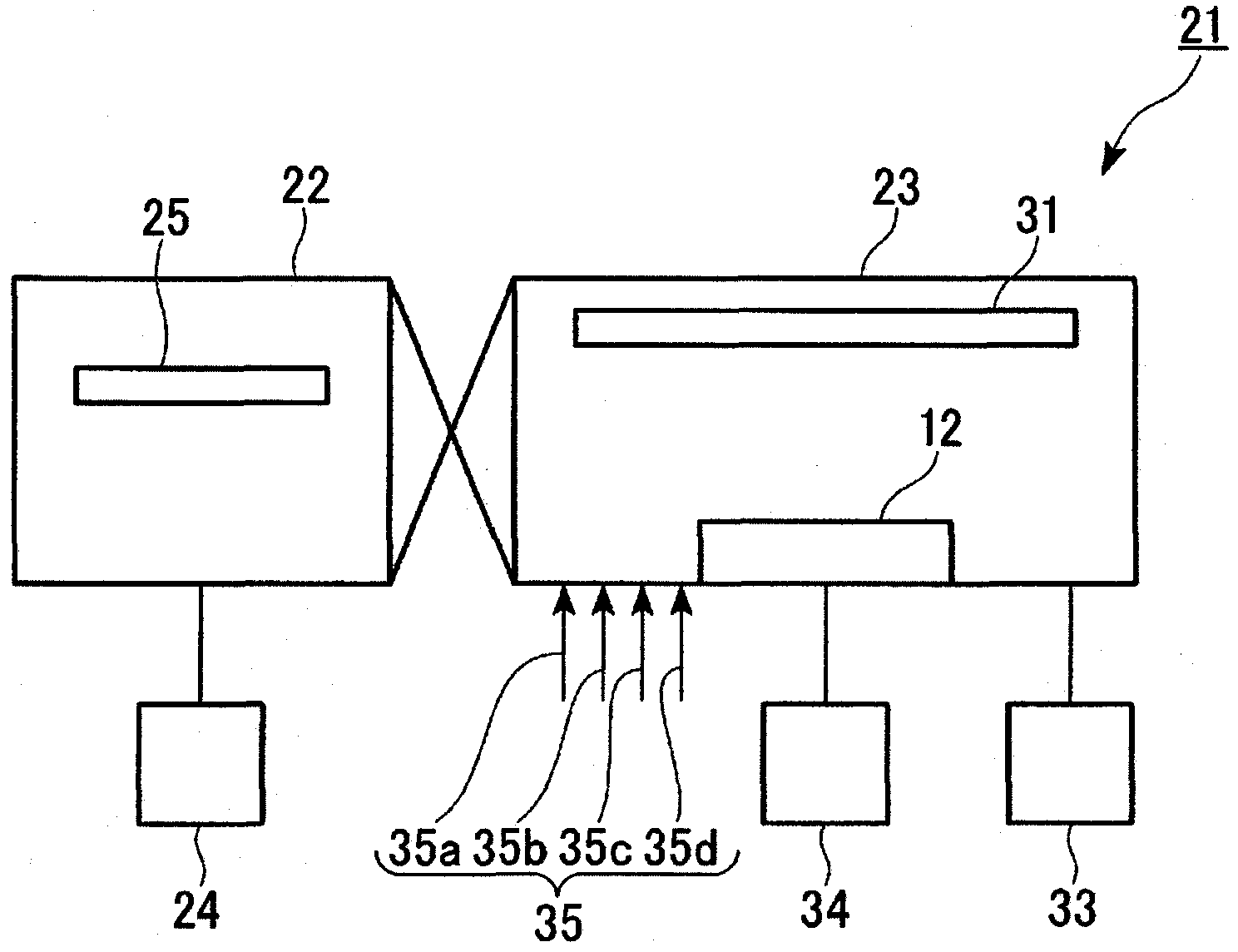
[0120] Figure 8 It is a sectional view of main parts showing a film forming chamber of a reciprocating magnetron sputtering device (film forming device) used for forming an antireflection film according to a second embodiment of the present invention.

[0121] The difference between this magnetron sputtering device 41 and the above-mentioned sputtering device 21 is that a side surface 23b of the film forming chamber 23 is vertically provided with a sputtering cathode mechanism (target sputtering cathode mechanism) which holds a target 27 of indium oxide-based material and generates a desired magnetic field. keep equipment)42.

[0122] The sputtering cathode mechanism 42 includes a rear plate 43 to which the target 27 is welded (fixed) with solder or the like, and a magnetic circuit (magnetic field generating device) 44 arranged along the back surface of the rear plate 43 . Magnetic circuit 44 is owing to produce horizontal magnetic field on the surface of target 27, so a plu...

no. 3 approach

[0128] Figure 9 It is a schematic configuration diagram showing a rotary sputtering apparatus according to a third embodiment of the present invention.

[0129] In the film formation chamber (vacuum container) 52 of the sputtering apparatus 51, the rotating body 54 which rotates about the center axis|shaft of this film formation chamber 52 is provided. On the outer peripheral surface of the rotating body 54, a substrate rack 53 ( Figure 9 in 4). Furthermore, on the inner surface of the film forming chamber 52, a plurality of cathodes 32 ( Figure 9 in 2). When the rotating body 54 is rotated about its axis and stopped at a position where the substrate holder 53 faces the cathode 32 , the substrate 26 supported by the substrate holder 53 of the rotating body 54 faces the target 27 held by the cathode 32 .

[0130] The film forming chamber 52 is provided with a device which divides the chamber into two sputtering regions S 1 , S 2 The partition plate 55. In both sputter...


PUM

PropertyMeasurementUnit
electrical resistivityaaaaaaaaaa
thicknessaaaaaaaaaa
thicknessaaaaaaaaaa

Abstract

Disclosed is a method for forming an antireflective film having a first indium-based oxide thin film and a second indium-based oxide thin film stacked on this first indium-based oxide thin film, and comprising: a first film formation step wherein a first indium-based oxide thin film is formed by sputtering using a first indium-based oxide target in a first reactive gas that contains one, two, or three selected from a group comprising oxygen gas, hydrogen gas, and water vapor; and a second film formation step wherein a second indium-based oxide thin film is formed on the first indium-based oxide thin film by sputtering using a second indium-based oxide target in a second reactive gas that contains one, two, or three selected from a group comprising oxygen gas, hydrogen gas, and water vapor and that has a different composition from the first reactive gas.

Description

technical field [0001] The present invention relates to a film forming method of an antireflection film, an antireflection film and a film forming apparatus, and more specifically, to a display surface suitable for a flat panel display (FPD), an operation surface such as a touch panel, and a light-receiving surface of a solar cell. A method for forming an anti-reflection film on a surface, etc., an anti-reflection film and a film-forming device. [0002] This application claims priority based on Japanese Patent Application No. 2008-268769 filed in Japan on October 17, 2008, the contents of which are incorporated herein by reference. Background technique [0003] In recent years, various antireflection films are used for antireflection in flat panel displays (FPDs), touch panels, solar cells, and the like. [0004] As an antireflection film conventionally used, an antireflection film having a multilayer structure in which a high-refractive index layer and a low-refractive in...

Claims


Application Information

Patent Timeline
Patent Type & Authority Applications(China)
IPC IPC(8): G02B1/11B32B7/02B32B9/00C23C14/08
CPCC23C14/086G02B1/113C23C14/3492G02F1/133502
Inventor 高桥明久石桥晓山本治彦柳坪秀典
Owner ULVAC INC
Why Eureka
Try Eureka