Wafer grinding device

A grinding device and wafer technology, which is applied in the field of optoelectronic information, can solve the problems of surface roughness, flatness, and wafer thickness tolerances that cannot meet the processing of patterned substrate wafers, high efficiency and low cost, and easy chipping at the edge of the wafer, etc., to achieve grinding The effect of long process time, balanced grinding time, and improved grinding efficiency

Active Publication Date: 2011-08-24
青岛华芯晶电科技有限公司
View PDF9 Cites 18 Cited by
  • Summary
  • Abstract
  • Description
  • Claims
  • Application Information

AI Technical Summary

Problems solved by technology

[0004] A common problem of wafers processed by traditional wafer grinding equipment is that the edge of the wafer is easy to sag.
The reason for this problem is that the grinding path rules cause the edge to wear more than the inside and easily form a sag
The qualified rate of the finished product obtained by the grinding device of the sapphire substrate in the prior art is low, and the long processing time results in poor efficiency and high cost, and the indicators such as surface roughness, flatness, and wafer thickness tolerance cannot reach the processing patterned substrate wafer. requirements

Method used


Image

  • Wafer grinding device
  • Wafer grinding device
  • Wafer grinding device

Examples


Embodiment Construction

[0022] The present invention will be described below with reference to the drawings.

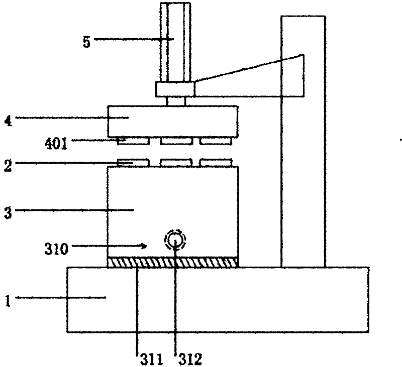
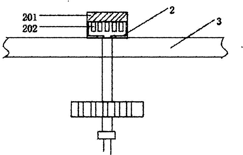
[0023] See figure 1 , The present invention includes a base 1, which is used to support the components of the grinding device; a wafer carrier 2, which is used to fix and hold the wafer 201; a workbench 3, which is used to support the wafer carrier 2 and is installed on the base 1. The grinding mechanism 4, which is used to grind the wafer 201, is located above the table 3; the pressure mechanism 5, which is used to apply pressure to the grinding head 401, is located above the grinding mechanism 4, and the pressure mechanism 5 adopts Air pressure device.

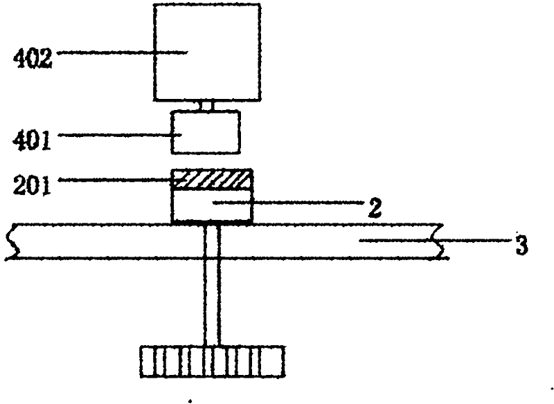
[0024] See figure 2 with Figure 5 The grinding mechanism 4 includes a grinding head 401, a driving motor 402 arranged above the grinding head 401 and used for driving the grinding head 401 to generate a rotational movement, and a coupling member 403 for fixing the grinding head 401. The connecting component 403 includes a movable support 404...


PUM


Abstract

The invention relates to a wafer grinding device for sapphire lining wafers. The invention provides a wafer grinding device which has high efficiency and avoids wafer edge collapse. The wafer grinding device comprises a base, a wafer carrier, a workbench, a grinding mechanism and a pressing mechanism, wherein the base is used for supporting components of the grinding device; the wafer carrier is used for fixing and holding the wafer; the workbench is used for supporting the wafer carrier and is installed on the base and comprises a first drive mechanism and a second drive mechanism, the first drive mechanism drives the workbench to do traverse and vertical reciprocation motion, and the second drive mechanism drives the wafer carrier to spin; the grinding mechanism is positioned above the workbench for grinding wafers and comprises a grinding head, a drive motor and a connection part, the drive motor drives the grinding mechanism to spin, and the connection part is used for fixing the grinding head; and the pressing mechanism is positioned above the grinding mechanism for applying a press onto the grinding head. The wafer grinding device basically eliminates the phenomenon of product edge collapse, and uses a single grinding head to grind a single wafer instead of multiple wafers adhered to the wafer carrier, so grinding efficiency is greatly improved.

Description

Technical field [0001] The present invention relates to the field of optoelectronic information technology, in particular to a wafer polishing device for a sapphire substrate wafer. Background technique [0002] The advantages of sapphire wafers as substrate materials: Sapphire is a single crystal material of aluminum oxide with very high hardness. It is a commonly used substrate material in the LED industry. It is used as a substrate for epitaxial growth such as gallium nitride. Production of blue light and other light-emitting diodes. Substrate processing is a major problem in the LED industry chain. It not only needs to achieve very high accuracy, especially the substrate used to make patterned wafers, the flatness (TTV) is required to be less than 5 microns, and the edge ring is less than 30 microns. , To achieve higher processing efficiency and a certain degree of economy. [0003] Sapphire is difficult to machine due to its high hardness and brittleness, and sapphire is the...

Claims


Application Information

Patent Timeline
Patent Type & Authority Applications(China)
IPC IPC(8): B24B37/04
Inventor 奚耀华夏澍
Owner 青岛华芯晶电科技有限公司
Why Eureka
Try Eureka