Differential amplifier architecture adapted to input level conversion
An input level, amplifier technology, applied in the field of source amplifier architecture, can solve the problems of increasing peak-to-peak voltage variation, difficult to achieve driving voltage accuracy, etc., to achieve the effect of improving peak-to-peak voltage variation
- Summary
- Abstract
- Description
- Claims
- Application Information
AI Technical Summary
Problems solved by technology
Method used
Image

Examples
no. 1 example
[0060] Figure 5A is a block diagram showing an exemplary configuration of the liquid crystal display device in the first embodiment of the present invention. The liquid crystal display device of this embodiment is provided with a source driver 100 , a gate driver 200 and a liquid crystal display panel 300 . The source driver 100 drives source electrodes (data lines) in the liquid crystal display panel 300 . The gate driver 200 drives gate electrodes (gate lines) in the liquid crystal display panel 300 . In the liquid crystal display panel 300, pixels are provided at respective intersections of source electrodes and gate electrodes.
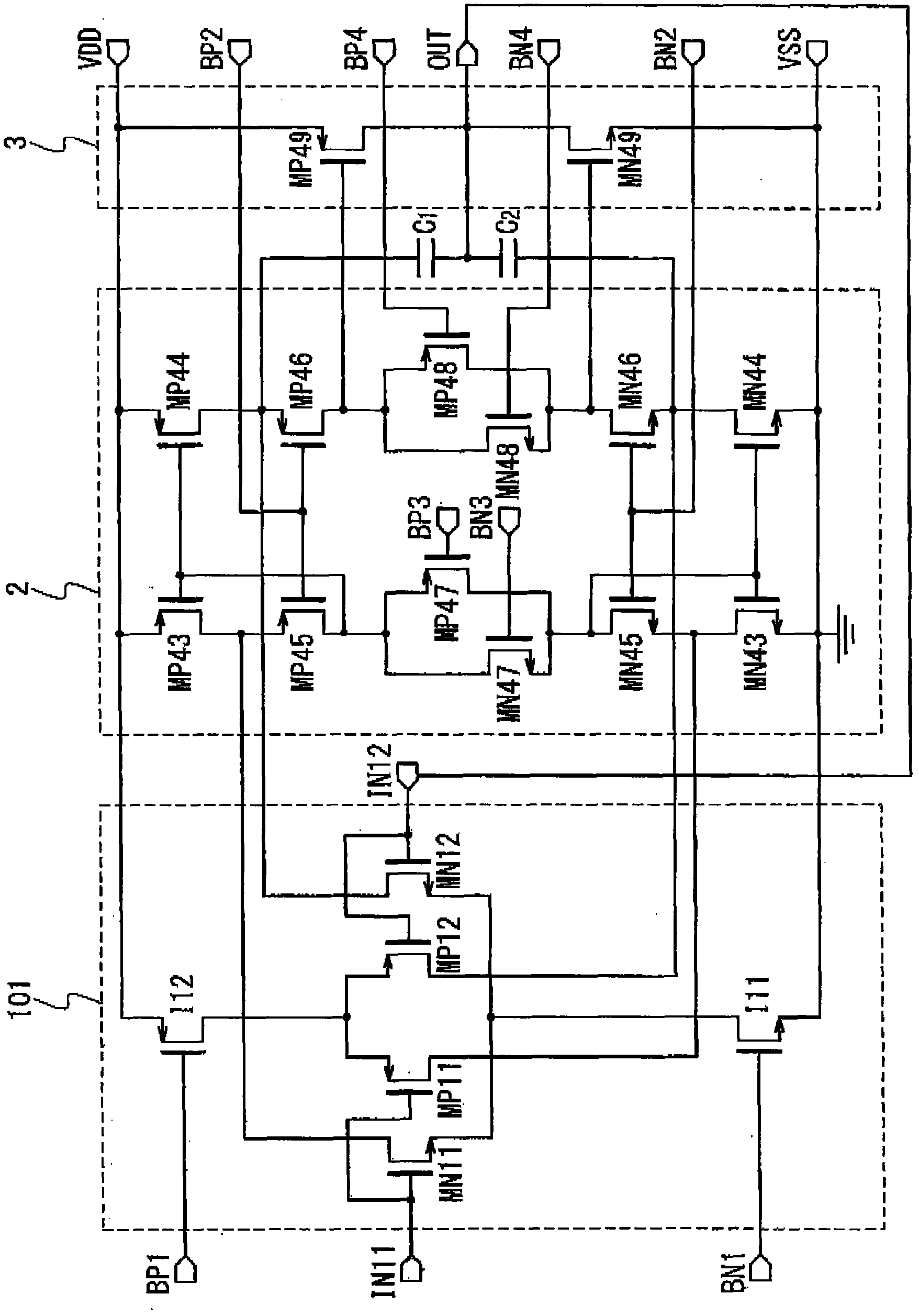
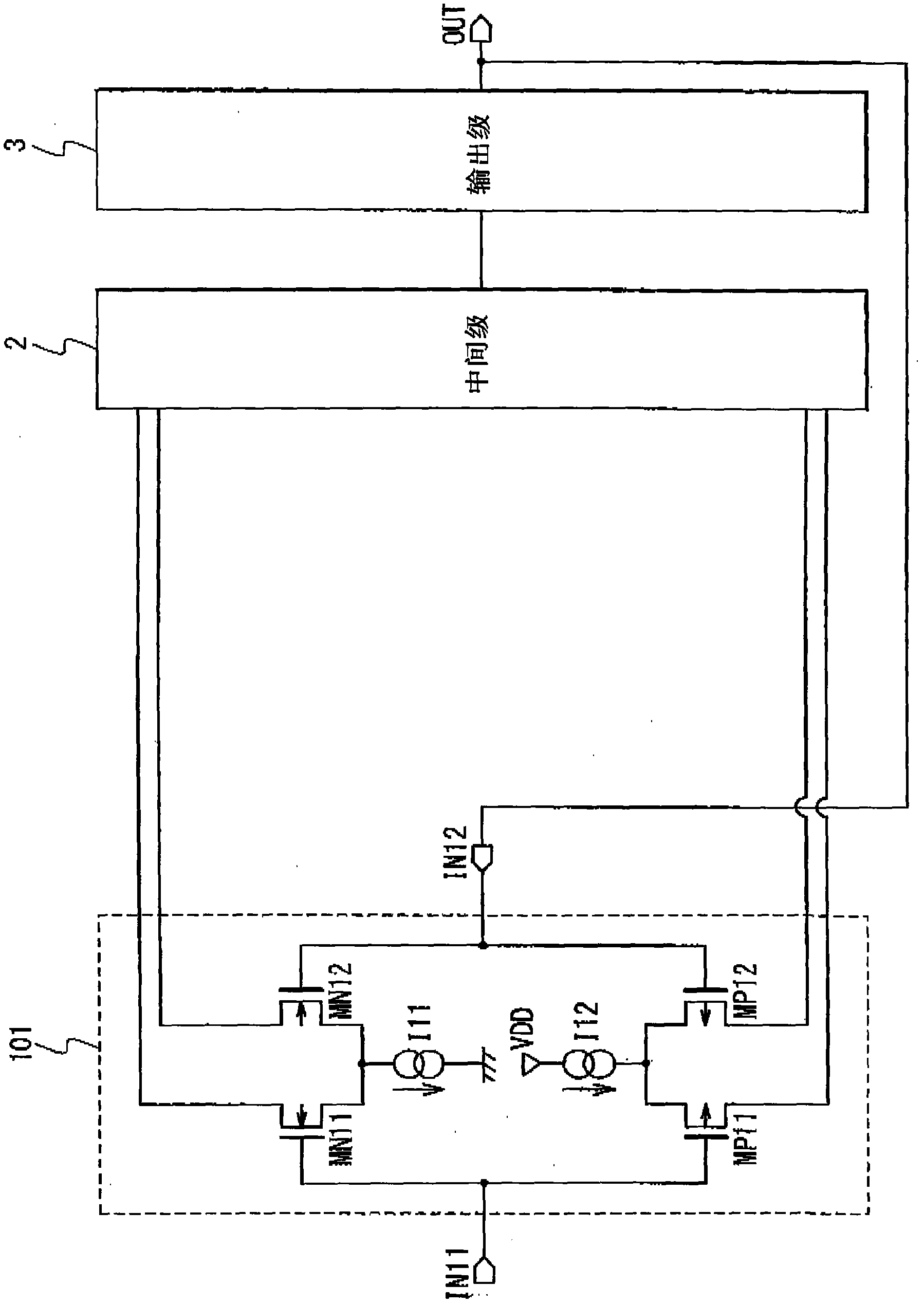
[0061] Figure 5B is a block diagram showing an exemplary configuration of the source driver 100 in the first embodiment. Figure 5B A circuit portion of the source driver 100 that drives two source electrodes (data lines) in the liquid crystal display panel 300 is shown.
[0062] The source driver 100 is provided with a latch 21 , a level s...
no. 2 example
[0101] Figure 9A is a circuit diagram showing an exemplary configuration of the source driver 100A in the second embodiment of the present invention, and Figure 9B is a circuit diagram showing an exemplary configuration of the source amplifier 25A in the second embodiment. In the second embodiment, the source driver 100A and the source amplifier 25A integrated therein are configured to provide input level shifting only in a voltage range close to the negative power supply voltage VSS and the positive power supply voltage VDD; No input level shifting is provided in the mid-voltage range.
[0102] Specifically, such as Figure 9A As shown in , the source driver 100A is provided with a switch control circuit 26 . The switch control circuit 26 responds to the pixel data D latched by the latch 21 IN The sum polarity signal POL generates a switch control signal SW_CTRL for controlling input switches SW21 and SW22 in input stage 1A in source amplifier 25A.
[0103] The source ...
no. 3 example
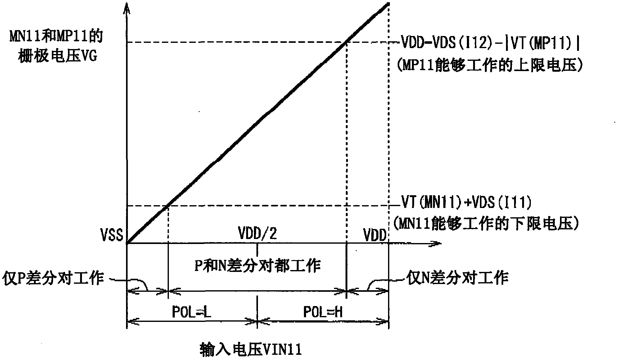
[0120] Figure 11 is a circuit diagram showing an exemplary configuration of a source amplifier in a source driver of a third embodiment of the present invention. The source amplifier 25B of the third embodiment is configured similarly to the source amplifier 25 of the first embodiment. The most important difference is that the NMOS differential pair of input stage 1B consists of depletion mode NMOS transistors MN31 and MN32. A depletion-mode transistor has a lower threshold voltage than an enhancement-mode transistor. The present embodiment is described assuming that the threshold voltage of the depletion transistor is adjusted to -0.1V; the threshold voltage of the depletion transistor can vary from 0.2V to 0V.
[0121] It should be noted here that even when the input voltage is the negative power supply voltage VSS, the NMOS differential pair formed by the depletion NMOS transistors MN31 and MN32 can operate. In this embodiment, both the NMOS differential pair and the PM...
PUM
 Abstract
Description
Claims
Application Information
 - R&D
- Intellectual Property
- Life Sciences
- Materials
- Tech Scout
- Unparalleled Data Quality
- Higher Quality Content
- 60% Fewer Hallucinations
Browse by: Latest US Patents, China's latest patents, Technical Efficacy Thesaurus, Application Domain, Technology Topic, Popular Technical Reports.
© 2025 PatSnap. All rights reserved.Legal|Privacy policy|Modern Slavery Act Transparency Statement|Sitemap|About US| Contact US: help@patsnap.com