Process for producing ceramic mobile phone circuit board
A production process and circuit board technology, applied in printed circuit, multi-layer circuit manufacturing, printed circuit manufacturing, etc., can solve the problems of smooth surface and poor bonding force of semi-cured resin, easy separation layer, conductive point displacement, etc. Achieve the effect of saving grinding equipment and grinding materials, enhancing the bonding force, and increasing the expansion and contraction space
- Summary
- Abstract
- Description
- Claims
- Application Information
AI Technical Summary
Problems solved by technology
Method used
Image

Examples
Embodiment 1
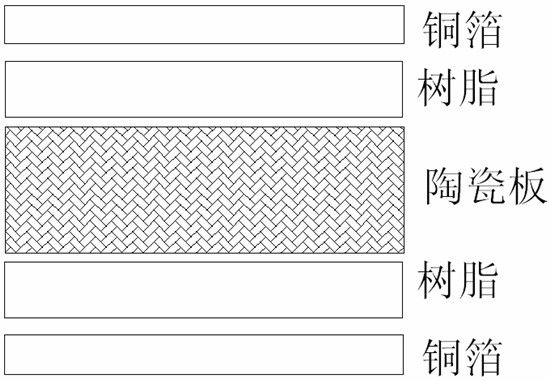
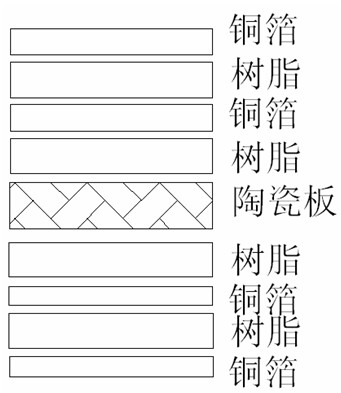
[0044] 1) Cut the ceramic plate, insulating resin and copper foil with a thickness of 0.2mm to the same size, roughen the surface of the ceramic plate with 10% sulfuric acid in mass percent concentration, wash and dry, and dry the copper foil, insulating resin, ceramic The board, insulating resin, and copper foil are stacked in sequence, and sent to a vacuum laminating machine for vacuum lamination to form a ceramic substrate. The lamination temperature is 240°C, the vacuum degree is -95KPA, and the lamination pressure is 30kg / in. 2 , the pressing time is 180 minutes;
[0045] 2) On the CNC machine tool, the spindle head is positioned in the plane, and the ceramic substrate is drilled with a micro drill. The positioning speed is 55m / min, the drill speed is 10m / min, and the diameter of the via hole is 0.3mm;
[0046] 3) After grinding, degreasing, micro-etching, pickling, water washing, and drying the ceramic substrate, hang the ceramic substrate in the electroplating solution,...
Embodiment 2
[0059] 1) Cut the ceramic board, insulating resin and copper foil with a thickness of 0.7mm to the same size, roughen the surface of the ceramic board with sulfuric acid with a concentration of 10% by mass, wash and dry the copper foil, insulating resin, ceramic The board, insulating resin, and copper foil are stacked in sequence, and sent to a vacuum lamination machine for vacuum lamination to form a ceramic substrate. The lamination temperature is 280°C, the vacuum degree is -90 KPA, and the lamination pressure is 35kg / in. 2 , the pressing time is 180 minutes;
[0060] 2) On the CNC machine tool, the spindle head is positioned in the plane, and the ceramic substrate is drilled with a micro drill. The positioning speed is 60m / min, the drill speed is 12m / min, and the diameter of the via hole is 0.3mm;
[0061] 3) After grinding, degreasing, micro-etching, pickling, water washing, and drying the ceramic substrate, hang the ceramic substrate in the electroplating solution, stir ...
PUM
| Property | Measurement | Unit |
|---|---|---|
| Thickness | aaaaa | aaaaa |
| Thickness | aaaaa | aaaaa |
Abstract
Description
Claims
Application Information
 - Generate Ideas
- Intellectual Property
- Life Sciences
- Materials
- Tech Scout
- Unparalleled Data Quality
- Higher Quality Content
- 60% Fewer Hallucinations
Browse by: Latest US Patents, China's latest patents, Technical Efficacy Thesaurus, Application Domain, Technology Topic, Popular Technical Reports.
© 2025 PatSnap. All rights reserved.Legal|Privacy policy|Modern Slavery Act Transparency Statement|Sitemap|About US| Contact US: help@patsnap.com