

Manufacturing method of LED chip
A technology of LED chip and manufacturing method, which is applied in the direction of electrical components, circuits, semiconductor devices, etc., can solve the problems of high masking layer requirements, device damage, and affecting the connection of LED chips, and achieve simple process, easy realization, and solution to fracture problems Effect
- Summary
- Abstract
- Description
- Claims
- Application Information
AI Technical Summary
Problems solved by technology
Method used
Image

Examples
Embodiment 1
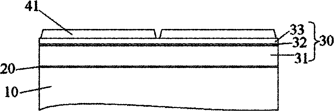
[0033] Provide a sapphire substrate, form a buffer layer on the substrate; form an epitaxial layer on the buffer layer, specifically comprising the following steps: forming a first semiconductor layer on the buffer layer, forming a light emitting layer on the first semiconductor layer, and forming a second semiconductor layer on the luminescent layer. A first mask layer is formed on the epitaxial layer after surface cleaning, and a first gap with a width of 10 μm is reserved between units of the first mask layer according to the design. Wherein, the material of the mask layer may be photoresist.
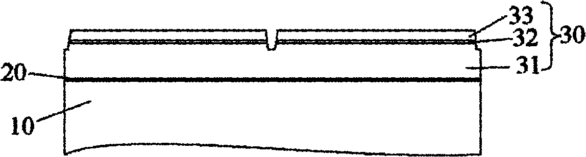
[0034] The second semiconductor layer, light-emitting layer, and part of the first semiconductor layer at the first gap position are removed by ICP, a first groove with a depth of 2 μm is formed on the epitaxial layer, and the first mask layer is removed.
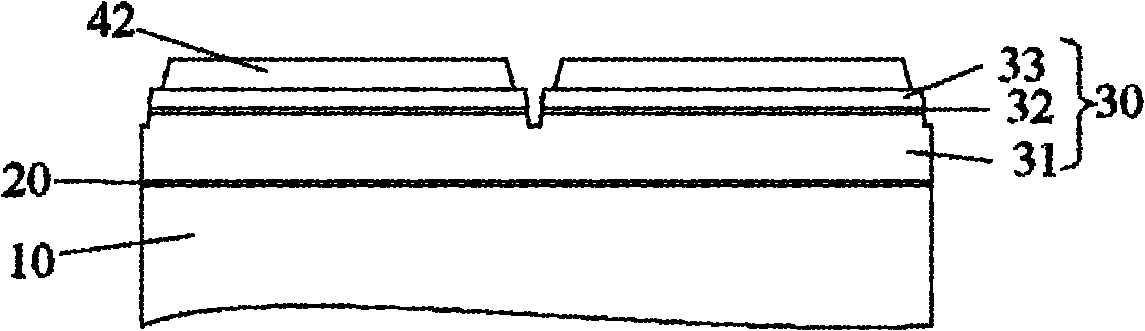
[0035] Formed on the epitaxial layer, a second mask layer is formed, the size of the second mask layer is limited within the ou...
Embodiment 2
[0041] A sapphire substrate is provided; a buffer layer is formed on the substrate, and an epitaxial layer is formed on the buffer layer, specifically comprising the following steps: forming a first semiconductor layer on the buffer layer, forming a light emitting layer on the first semiconductor layer, and forming a second semiconductor layer on the luminescent layer. The rest of the operation method is the same as that of Embodiment 1, except that the width of the first gap is 15 μm, the first groove with a depth of 3 μm is formed on the epitaxial layer, and the edge of the second mask layer is retracted by 15 μm from the first mask layer. The second ICP etching, the depth is 3 μm, the edge of the third mask layer is 15 μm inward than the second mask layer, the third ICP etching, the depth is 1.5 μm, and the thickness of the electrical insulating layer is 8000 angstroms.
PUM
| Property | Measurement | Unit |
|---|---|---|
| Depth | aaaaa | aaaaa |
| Depth | aaaaa | aaaaa |
| Thickness | aaaaa | aaaaa |
Abstract
Description
Claims
Application Information