Preparation method for copper oxide nano line array film

A technology of copper oxide nanowires and copper thin films, applied in ion implantation plating, metal material coating process, coating and other directions, can solve problems such as poor controllability and limited substrate materials, and expand the application field and scope , Flexible preparation and good controllability

Inactive Publication Date: 2011-09-14
HENAN UNIVERSITY
View PDF3 Cites 18 Cited by
  • Summary
  • Abstract
  • Description
  • Claims
  • Application Information

AI Technical Summary

Problems solved by technology

[0004] The purpose of the present invention is to provide a method for preparing a copper oxide nanowire array film, so as to overcome the disadvantages of poor controllability and limitation of the substrate material in the current preparation method

Method used


Image

  • Preparation method for copper oxide nano line array film
  • Preparation method for copper oxide nano line array film
  • Preparation method for copper oxide nano line array film

Examples


Embodiment 1

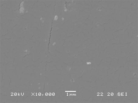
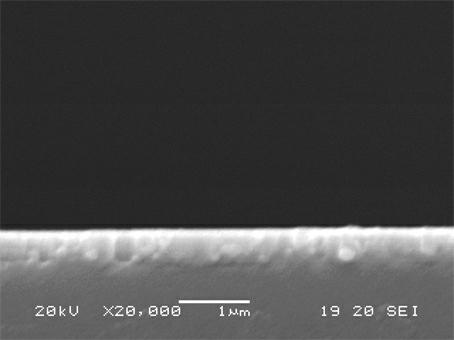
[0026] (1) After putting the copper target with a purity of 99.99% and the cleaned FTO into the sputtering chamber, first use a mechanical pump and a molecular pump to pump the vacuum of the sputtering chamber to 3.0×10 -3 Pa, then filled with argon gas with a purity ≥ 99.999%, the flow rate was 23 sccm, the main valve was adjusted to keep the vacuum at 0.35Pa, the current was adjusted to 0.25A, the voltage was 300V, the substrate speed was 13 r / min, and the sputtering Time 10min, obtain about 500 nanometers thick metal copper film, characterization sees figure 1 and figure 2 .

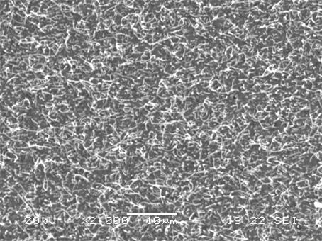
[0027] (2) Put the metal copper film obtained in step (1) into a tube furnace quickly, the tube mouth of the tube furnace close to the sample end is closed, and the other end is connected to the atmosphere; the heating rate is 20°C / min, in the atmosphere After annealing at 500°C for 8 hours, a vertically grown copper oxide nanowire array film was obtained. See the attached Figure 3-6 .

Embodiment 2

[0029] 1) After putting the copper target with a purity of 99.99% and the cleaned FTO into the sputtering chamber, first use a mechanical pump and a molecular pump to pump the vacuum of the sputtering chamber to 4×10 -3 Pa, then filled with argon gas with a purity ≥ 99.999%, the flow rate was 20 sccm, and the main valve was adjusted to keep the vacuum at 3.0×10 -1 Pa, adjust the current to be 0.2A, the voltage to be 350V, and the sputtering time to be 30min to obtain a metal copper film with a thickness of about 1.2μm;

[0030] (2) Put the metal copper film obtained in step (1) into a tube furnace quickly, the tube mouth of the tube furnace close to the sample end is closed, and the other end is connected to the atmosphere; the heating rate is 20°C / min, in the atmosphere After annealing at 450° C. for 10 hours, a vertically grown copper oxide nanowire array film is obtained.


PUM

PropertyMeasurementUnit
thicknessaaaaaaaaaa

Abstract

The invention belongs to low-dimensional nano material preparation and application field of nano technology, and particularly relates to a preparation method for a copper oxide nano line array film. The preparation method comprises the following steps: sputtering a metal copper film on an FTO substrate by adopting a magnetron sputter plating method, and then annealing the prepared film under air atmosphere, thus obtaining the copper oxide nano line array film. In the preparation method, the controllability is good, the preparation is flexible, the preparation method is not limited to prepare substrate materials, the scale production in the industry can be conducted conveniently, and the application field and scope of nano line array film can be expanded to a greater degree.

Description

technical field [0001] The invention belongs to the fields of preparation of low-dimensional nanometer materials and application of nanotechnology, and in particular relates to a method for preparing a copper oxide nanowire array thin film. Background technique [0002] Among the metal oxides, most of them are n-type semiconductors, and CuO is one of the few p-type semiconductor materials, because CuO can be used in various fields such as ferromagnetic materials, high-temperature superconductivity, battery electrodes, and gas sensors. , and thus has received widespread attention. Compared with traditional bulk materials, one-dimensional nanowire materials have superior performance in the field of nanotechnology due to their small size effect and large specific surface area, and have attracted more and more attention and research. Among them, the preparation method and application technology of low-dimensional nanowire materials are the current research hotspot and focus. ...

Claims


Application Information

Patent Timeline
Patent Type & Authority Applications(China)
IPC IPC(8): C23C14/18C23C14/35C23C14/58
Inventor 杜祖亮乔振聪程轲程纲
Owner HENAN UNIVERSITY
Why Eureka
Try Eureka