Method for measuring temperature by using thermal wave meter

A technology for measuring temperature and thermal wave instrument, which is applied in semiconductor/solid-state device testing/measurement, electrical components, semiconductor/solid-state device manufacturing, etc. It can solve the problems of weak process simulation, time-consuming, inability to simulate, etc., and achieve process simulation Strong performance, wide application range and wide applicability

Inactive Publication Date: 2011-09-14
NO 771 INST OF NO 9 RES INST CHINA AEROSPACE SCI & TECH
View PDF1 Cites 6 Cited by
  • Summary
  • Abstract
  • Description
  • Claims
  • Application Information

AI Technical Summary

Problems solved by technology

[0003] (1) Time-consuming, TC Wafer calibration usually needs to manually put the Wafer in and lead out the wires
For closed chambers, it is necessary to shut down and open the chamber, especially for some high vacuum machines, vacuum reconstruction is required, which usually takes several hours, which is a big time-consuming in semiconductor production
[0004] (2) Poor applicability, due to the limitation of wires, some types of machines cannot use this method, such as vacuum chambers with high sealing requirements
[0005] (3) Process simulation is not strong
For most CVD (chemical vapor deposition) and PVD (physical vapor deposition) machines, only the set temperature can be simply measured, and the temperature during the process cannot be measured, because the processing of the process will affect the TCWafer In addition, the movement of Wafer in the Process Chamber cannot be simulated, such as the conversion between Chambers (PVD); the movement of Wafer in the film holder (such as the C1 chemical vapor deposition machine produced by Novellus Company), Movement of Wafer in process
[0006] (4) The cost is high; a piece of TC Wafer usually costs thousands of dollars

Method used


Image

  • Method for measuring temperature by using thermal wave meter
  • Method for measuring temperature by using thermal wave meter
  • Method for measuring temperature by using thermal wave meter

Examples


Embodiment Construction

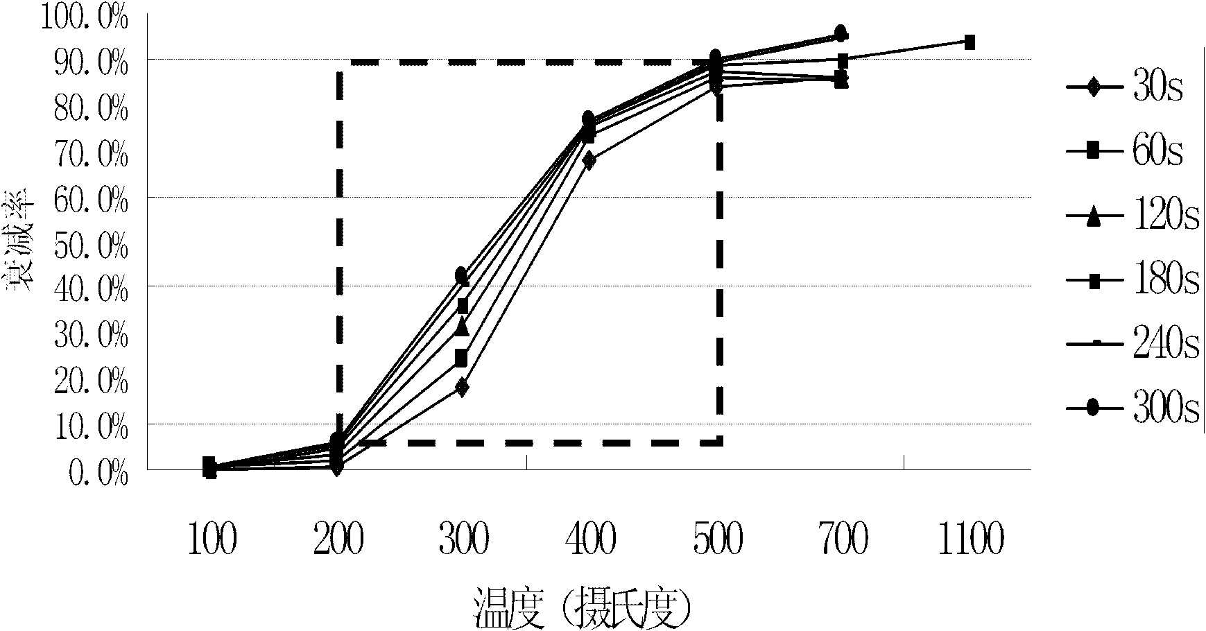
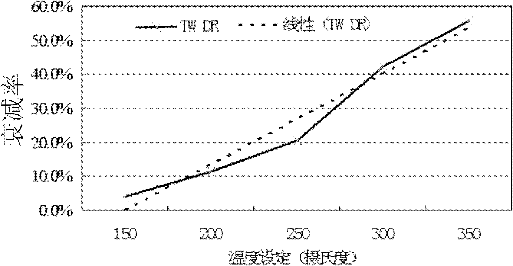
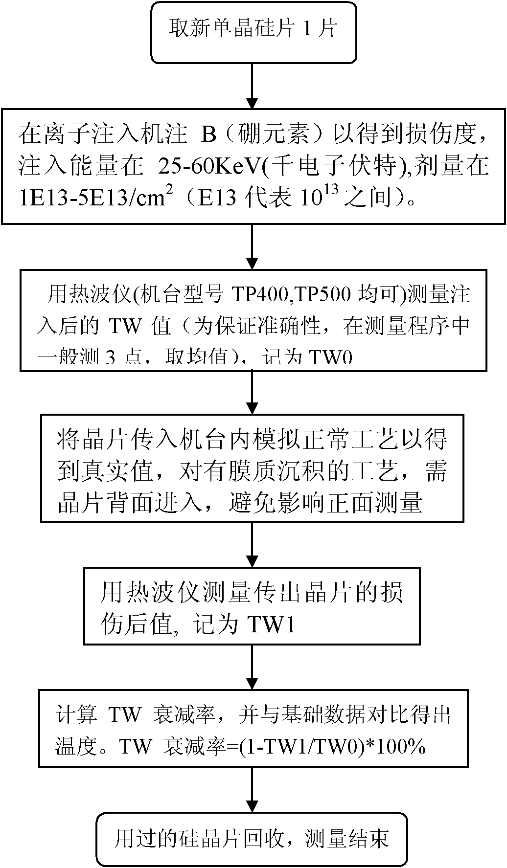
[0029] Below in conjunction with accompanying drawing, the present invention is described in further detail, and practical application example:

[0030] see figure 1 , a method for measuring temperature using a thermal wave instrument, the steps are as follows:

[0031] (1) Take a piece of silicon wafer, the type of wafer can be selected as P-TYPE (resistivity: 0.5-100ohm.cm).

[0032] (2) Inject B (boron element) into the ion implanter to obtain the damage degree, the implantation energy is 25-60KeV (kiloelectron volts), and the dose is 1E13-5E13 / cm 2 (E13 stands for 10 13 )between.

[0033] (3) measure the thermal wave signal value TW0 after injection with a thermal wave instrument;

[0034] (4) Pass the wafer into the machine (simulate the normal process to obtain the real value), so that the machine can work normally. When the machine is working, the temperature generated in the cavity will repair the damage of the inserted wafer. ; For processes with film deposition...


PUM


Abstract

The invention discloses a method for measuring temperature by using a thermal wave meter. In a semiconductor manufacturing process, a lattice structure of a monocrystalline silicon wafer is damaged by ion injection, and the damage threshold, called as TW (Thermal Wave) value, can be measured through the thermal wave meter. The damage of a lattice can be repaired after annealing at a certain temperature and then the TW value is reduced. More importantly, the degree of the reduction is directly related to the temperature. According to the relation, the injected monocrystalline silicon wafer is respectively measured before and after the monocrystalline silicon wafer enters a machine platform of which the temperature is to be measured, the prior valve is called as TW0 and the later valve is called as TW1; the decay rate is calculated according to the formula that: TW decay rate is equal to (1-TW1/TW0)*100%; the decay rate corresponds to a fixed temperature; and the temperature of wafer-accessed machine platform is obtained by comparing the fixed temperature and base data. The method has the advantages that: the operation is simple; the time is saved; the cost is low; the process imitativeness is high; the environment of the machine platform is not damaged; the adaptability is high; a film in a semiconductor factory can be etched; and the temperature of the alloy furnace tube machine platform can be measured.

Description

Technical field: [0001] The invention belongs to the field of semiconductors, and relates to a temperature measurement method, in particular to a temperature measurement method using a thermal wave instrument. Background technique: [0002] In semiconductor manufacturing, the process has strict requirements on the accuracy and stability of temperature, so the measurement and calibration of temperature is very important. The existing temperature measurement method mainly uses Thermal Couple (thermocouple) in addition to the temperature control module of the device itself. , hereinafter referred to as TC) Wafer (wafer), although this method can get a more accurate temperature, but there are some unavoidable shortcomings in practical applications: [0003] (1) Time-consuming, TC Wafer calibration usually requires manually putting the Wafer in and leading out the wires. For closed chambers, it is necessary to shut down and open the chamber, especially for some high vacuum machi...

Claims


Application Information

Patent Timeline
Patent Type & Authority Applications(China)
IPC IPC(8): H01L21/66H01L21/265
Inventor 张思申仲维续张晓雷贺金良
Owner NO 771 INST OF NO 9 RES INST CHINA AEROSPACE SCI & TECH
Why Eureka
Try Eureka