

Method for forming shallow trench isolation structure for flash memory
A technology of flash memory and isolation structure, applied in semiconductor/solid-state device manufacturing, electrical components, circuits, etc., can solve the problems of uneven thickness of polysilicon layer, achieve improved uniformity, short deposition time, and improved programming and erasing efficiency effect
- Summary
- Abstract
- Description
- Claims
- Application Information
AI Technical Summary
Problems solved by technology
Method used
Image

Examples
Embodiment Construction
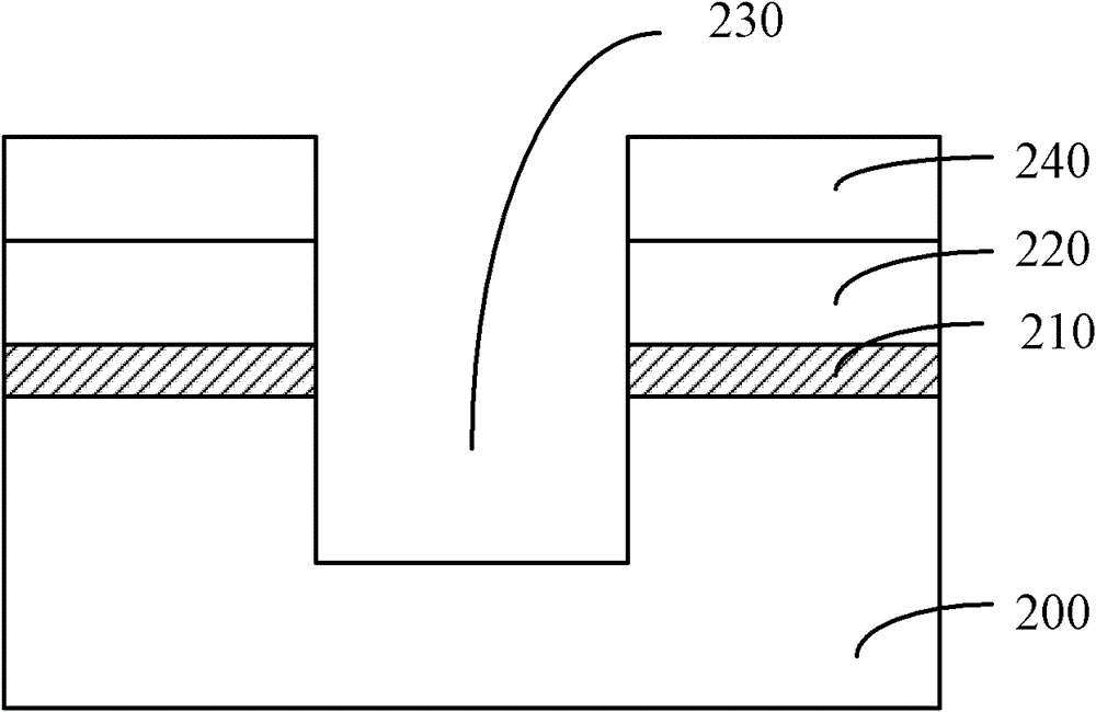
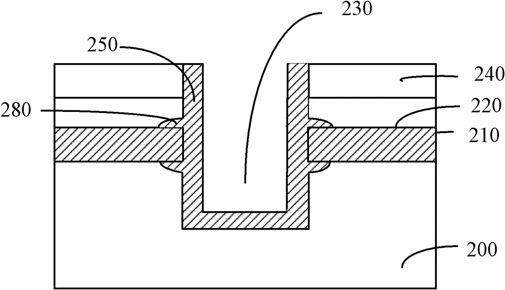
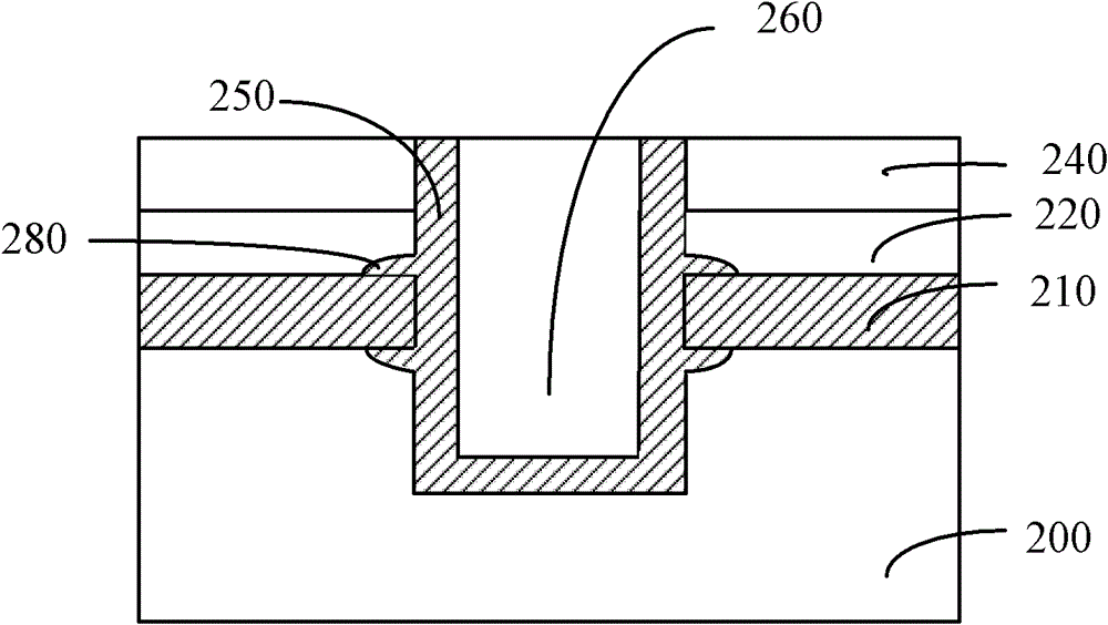
[0031] It can be seen from the background technology that the “smiley face” problem of the floating gate tunneling oxide caused by the formation of the shallow trench isolation pad oxygen layer in the existing flash memory reduces the coupling coefficient of the control gate and the source and drain to the floating gate, so that The programming and erasing efficiency of the device is reduced, and the read current of the device after erasing is reduced, and the working window of the storage device is reduced. The inventors of the present invention have studied the above problems and found that by changing the formation method of the isolation structure between adjacent flash memory cells in the flash memory, the read current of the flash memory can be reduced, and the efficiency of writing and erasing can be improved.
[0032] The inventor has conducted research on the above-mentioned problems, and believes that in the existing method for forming the isolation structure between ...
PUM
| Property | Measurement | Unit |
|---|---|---|
| thickness | aaaaa | aaaaa |
| thickness | aaaaa | aaaaa |
| thickness | aaaaa | aaaaa |
Abstract
Description
Claims
Application Information