Light-emitting diode and manufacturing method thereof

A technology for light-emitting diodes and a manufacturing method, which is applied to electrical components, circuits, semiconductor devices, etc., can solve the problems that the uniform current diffusion does not have an ideal effect, other properties of the material are reduced, and the uniform current diffusion does not play an obvious effect. , to achieve the effect of improving compliance efficiency, improving the ability to resist static electricity, and improving luminous brightness

Inactive Publication Date: 2011-09-14
ENRAYTEK OPTOELECTRONICS
View PDF5 Cites 15 Cited by
  • Summary
  • Abstract
  • Description
  • Claims
  • Application Information

AI Technical Summary

Problems solved by technology

[0004] CN101694858A patent proposes an LED epitaxial structure and its manufacturing method, the structure is inserted between the light-emitting layer and the p-type nitride layer by undoped Al x In y Ga 1-x-y n-layer and p-type Al x In y Ga 1-x-y The insertion layer composed of n layers alternately protects the ESD protection performance of the material, and does not reduce other properties o

Method used


Image

  • Light-emitting diode and manufacturing method thereof
  • Light-emitting diode and manufacturing method thereof
  • Light-emitting diode and manufacturing method thereof

Examples


Embodiment 1

[0026] In this embodiment, the light emitting diode is provided with a first insertion layer inside the n-type semiconductor layer, and a second insertion layer is provided between the n-type semiconductor layer and the active layer.

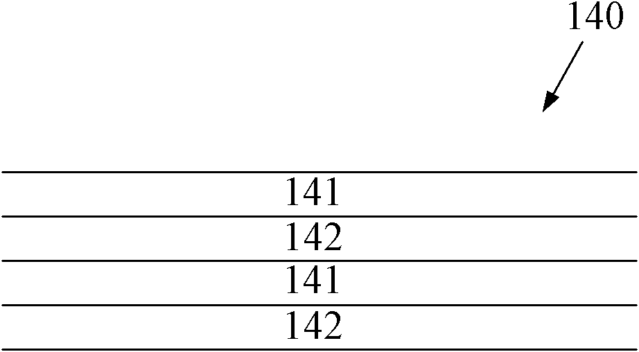
[0027] Please refer to figure 1 , Figure 2A and Figure 2B ,in, figure 1It is a schematic structural diagram of a light emitting diode according to Embodiment 1 of the present invention, Figure 2A for figure 1 A schematic diagram of the first insertion layer of the LED shown, Figure 2B for figure 1 Schematic of the second insertion layer of the LED shown.

[0028] Such as figure 1 As shown, taking a gallium nitride-based blue light diode as an example, the light emitting diode includes: a substrate 100; a buffer layer 110, an undoped layer 120, an n-type semiconductor layer 130, an active Layer 160, p-type semiconductor layer 170, and current spreading layer 180; in addition, the light emitting diode also includes a first insertion la...

Embodiment 2

[0043] The difference between this embodiment and the first embodiment is that the light emitting diode only has a first insertion layer inside the n-type semiconductor layer.

[0044] For details, please refer to image 3 , which is a schematic structural diagram of a light emitting diode according to Embodiment 2 of the present invention. The light emitting diode comprises: a substrate 200; a buffer layer 210, an undoped layer 220, an n-type semiconductor layer 230, an active layer 260, a p-type semiconductor layer 270, and a current diffusion layer 280 sequentially located on the substrate 200; In addition, the light emitting diode further includes a first insertion layer 240 disposed inside the n-type semiconductor layer 230, wherein the first insertion layer 240 is made of at least one layer of non-doped Al x In y Ga 1-x-y N layer and / or at least one layer of Si-doped Al x In y Ga 1-x-y Consists of N layers, where 0≤x<0.2, 0≤y<0.2. When current is injected into the...

Embodiment 3

[0047] The difference between this embodiment and the first embodiment is that the light emitting diode only has a second insertion layer between the n-type semiconductor layer and the active layer.

[0048] The light-emitting diode includes: a substrate; a buffer layer, a non-doped layer, an n-type semiconductor layer, an active layer, a p-type semiconductor layer, and a current diffusion layer sequentially located on the substrate; in addition, the light-emitting diode also includes A second insertion layer disposed between the n-type semiconductor layer and the active layer, the second insertion layer is composed of at least one layer of non-doped Al x In y Ga 1-x-y N layer and / or at least one layer of Si-doped Al x In y Ga 1-x-y N layers, where 0≤x<0.2, 0≤y<0.2. When current is injected into the n-type region, the second insertion layer can act as a buffer, preventing electrons from diffusing to the p-type region, improving the coincidence efficiency of electrons and ho...


PUM


Abstract

The invention discloses a light-emitting diode and a manufacturing method thereof. The light-emitting diode comprises a substrate, a buffering layer, a non-doped layer, an n type semiconductor layer, an active layer, a p type semiconductor layer, a current diffusion layer, a first insertion layer and/or a second insertion layer, wherein the buffering layer, the non-doped layer, the n type semiconductor layer, the active layer, the p type semiconductor layer and the current diffusion layer are positioned on the substrate; the first insertion layer is arranged in the n type semiconductor layer; and the second insertion layer is arranged between the n type semiconductor layer and the active layer. The first insertion layer and the second insertion layer consist of at least one layer of non-doped AlxInyGa1-x-yN layer and/or at least one layer of Si-doped AlxInyGa1-x-yN layer, wherein x and y are more than or equal to 0 and less than 0.2. When current is injected into an n type area, the insertion layers play a role of buffering to prevent electrons from diffusing into a p type area, so the conformity efficiency of the electrons and holes is improved and then the illumination brightness of the light-emitting diode is improved. In addition, the insertion layers can achieve the effect similar to charging and discharging, so the anti-static ability of materials is effectively improved.

Description

technical field [0001] The invention relates to the field of semiconductor light emitting, in particular to a light emitting diode and a manufacturing method thereof. Background technique [0002] Light Emitting Diode (LED, Light Emitting Diode) is used in various fields due to its advantages of long life and low energy consumption, especially as its lighting performance index is greatly improved day by day, LED is often used as a light emitting device in the lighting field. Among them, gallium nitride (GaN) is the representative III-V compound semiconductor due to its wide band gap, high luminous efficiency, high electron saturation drift speed, and stable chemical properties. The field of optoelectronic devices has great application potential and has attracted widespread attention. At present, the general LED structure adopts the direct growth of the current spreading layer (Spreading layer), such as indium gallium nitride layer (InGaN layer) or indium Tin oxide layer (I...

Claims


Application Information

Patent Timeline
IPC IPC(8): H01L33/02H01L33/14H01L33/00
Inventor 李淼
Owner ENRAYTEK OPTOELECTRONICS
Why Eureka
Try Eureka