Semiconductor film growth control device and semiconductor film growth control method

A technology for thin film growth and control equipment, applied in gaseous chemical plating, metal material coating process, coating and other directions, can solve the problems of uncontrollable thin film thickness of semiconductor materials, affecting device performance, and delaying valve switching, etc. Conducive to precise control, improve control accuracy, and reduce the effect of transition layer growth

Inactive Publication Date: 2011-10-05
广东众元半导体科技有限公司
View PDF1 Cites 7 Cited by
  • Summary
  • Abstract
  • Description
  • Claims
  • Application Information

AI Technical Summary

Problems solved by technology

Because a steep film interface is often required in thin film devices, such as the multi-quantum well structure in LED devices; the conventional reaction source switching method is far away from the reaction chamber because the switching valve position is far away, so that the actual chamber atmosphere switching is delayed after the valve switching , after the valve is closed, there is still residual reaction source gas in the intake pipe, and these gases then ent

Method used


Image

  • Semiconductor film growth control device and semiconductor film growth control method
  • Semiconductor film growth control device and semiconductor film growth control method
  • Semiconductor film growth control device and semiconductor film growth control method

Examples


Embodiment 1

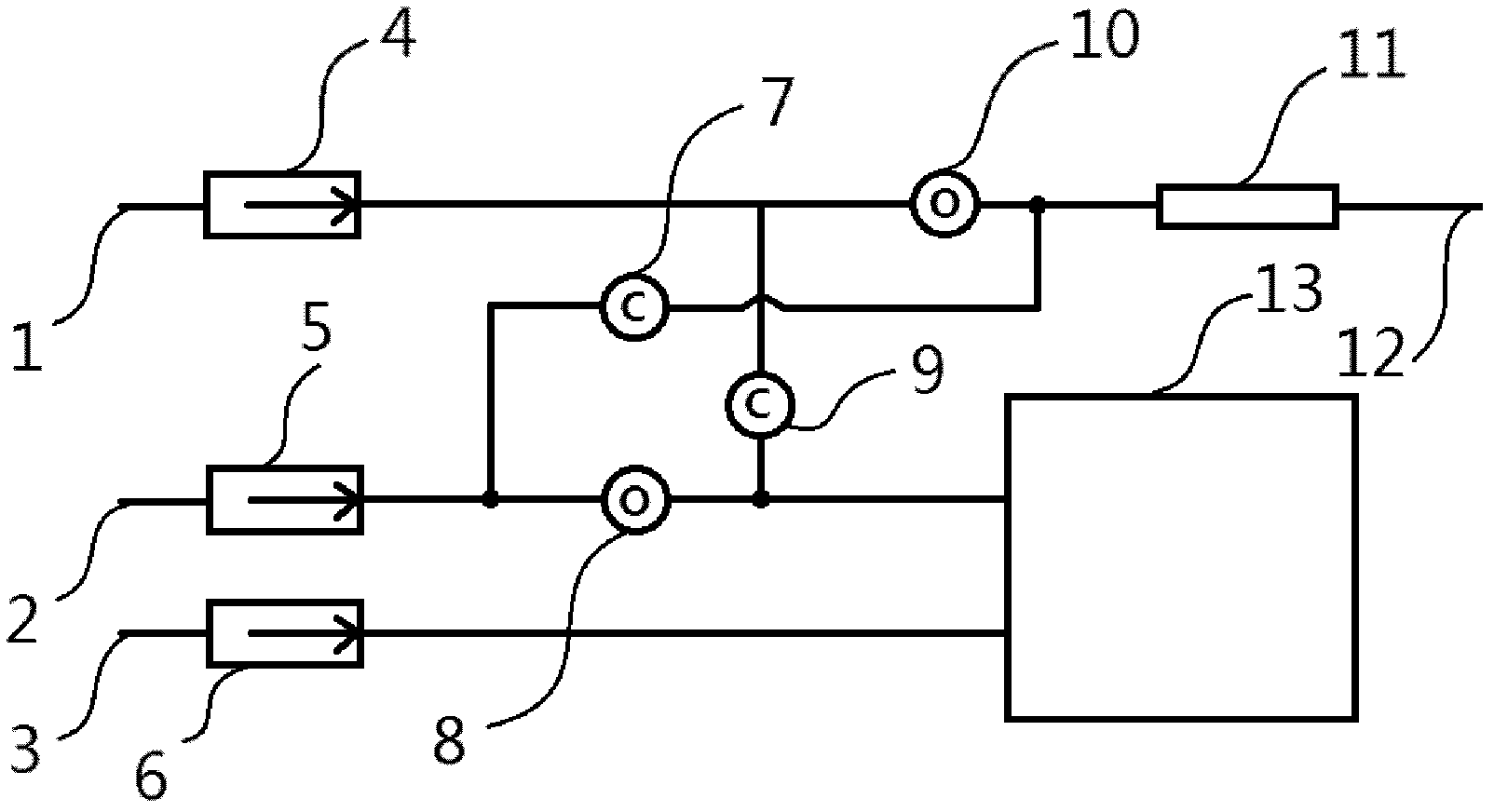
[0028] Such asfigure 1 As shown, in the first process stage, the first inlet pipe 1 is fed into the carrier gas hydrogen, the second inlet pipe is fed into the 2 reaction source trimethylgallium, and the third inlet pipe is fed into the 3 reaction source ammonia; One flow controller 4 is set to 10000 sccm, the second flow controller 5 is set to 10000 sccm, and the third flow controller 6 is set to 20000 sccm; the first branch valve 7 is closed, the second valve 8 is opened, and the second branch valve 9 is closed , the first valve 10 is opened; the trimethylgallium reaction source enters the semiconductor thin film growth reaction chamber 13, and the hydrogen gas enters the first tail gas pipeline 12 for gallium nitride thin film growth; in the second process stage, the first branch valve 7 is opened, The second valve 8 is closed at the same time, the second branch valve 9 is opened, and the first valve 10 is closed simultaneously; the trimethylgallium reaction source in the se...

Embodiment 2

[0030] Such as figure 1 As shown, in the first process stage, the first inlet pipe 1 is fed into the reaction source trimethylaluminum, the second inlet pipe 2 is fed into the reaction source trimethylgallium, and the third inlet pipe 3 is fed into the reaction source Ammonia. The first flow controller 4 is set to 10000 sccm, the second flow controller 5 is set to 10000 sccm, and the third flow controller 6 is set to 20000 sccm, while the first branch valve 7 is closed, the second valve 8 is opened, and the second branch valve 9 is closed, the first valve 10 is opened, trimethylgallium enters the semiconductor film growth reaction chamber 13, and trimethylaluminum enters the first tail gas pipeline 12 to perform gallium nitride film growth; in the second process stage, the first branch valve 7 is opened, the second valve 8 is closed simultaneously, the second branch valve 9 is opened simultaneously, the first valve 10 is closed simultaneously, the trimethylaluminum in the fir...

Embodiment 3

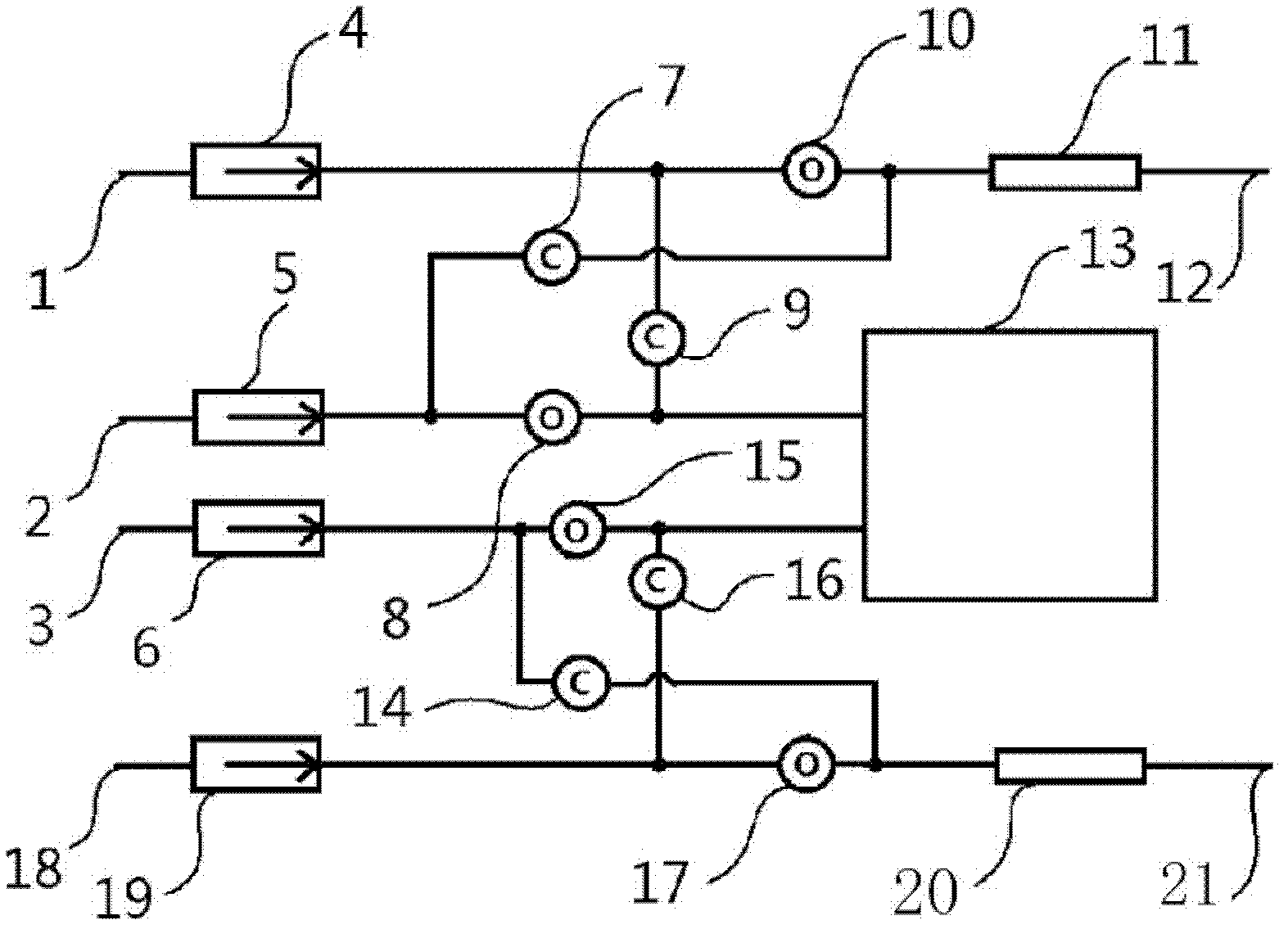
[0032] Such as figure 2 , in the first process stage, the first air intake pipe 1 feeds carrier gas hydrogen, the second air intake pipe feeds 2 reaction source trimethylgallium, the third air intake pipe 3 feeds reaction source ammonia; the fourth road Inlet pipeline 18 feeds hydrogen, the first flow controller 4 is set to 10000sccm, the second flow controller 5 is set to 10000sccm, the third flow controller 6 is set to 20000sccm, and the fourth flow controller 19 is set to 20000sccm; A branch valve 7 is opened, the second valve 8 is opened, the second branch valve 9 is closed, the first valve 10 is opened, the third branch valve 14 is closed, the third valve 15 is opened, the fourth branch valve 16 is closed, and the fourth branch valve is closed. The valve 17 is opened, trimethylgallium and ammonia gas enter the semiconductor film growth reaction chamber 13, and hydrogen gas enters the first tail gas pipeline 12 and the second tail gas pipeline 21 to grow gallium nitride f...


PUM


Abstract

The invention particularly relates to a semiconductor film growth control device and a semiconductor film growth control method using the same. The semiconductor film growth control device provided by the invention comprises a response source pipeline and a semiconductor film growth response cavity, wherein the response source pipeline comprises a plurality of intake pipes; each intake pipe is provided with a valve and a flow controller; and the valve is arranged in a position adjacent to the semiconductor film growth response cavity. When the semiconductor film growth control device is used for preparing semiconductor film materials, since the valve is near enough to semiconductor film growth response cavity, the response source and carrier gas can be quickly switched to enter the response cavity, and the film growth can be quickly stopped or started, thereby implementing accurate control of film thickness. The invention can also implement quickly switching among different response gas atmospheres to reduce the growth of the transition layer, thereby implementing the steep growth interface between films of different components and greatly improving the properties of the film devices.

Description

[0001] technical field [0002] The present invention relates to a semiconductor growth device, in particular to a device for controlling the growth of a semiconductor thin film and a method for controlling the growth of a semiconductor thin film using the device, which is used for precise transportation of reaction sources of semiconductor manufacturing equipment, especially metal organic chemical vapor deposition equipment (MOCVD) source delivery control system. Background technique [0003] The study of semiconductor thin film materials mainly depends on the preparation methods of semiconductor thin films. High-quality semiconductor thin film materials are conducive to the research of thin film device physics and the development of thin film device applications. In vapor phase thin film manufacturing equipment, especially in the growth process, it is often necessary to switch the concentration and composition ratio of the growth source gas multiple times to prepare a mult...

Claims


Application Information

Patent Timeline
IPC IPC(8): C23C16/455C23C16/52
Inventor 甘志银严晗朱海科王亮
Owner 广东众元半导体科技有限公司
Why Eureka
Try Eureka