Planar spiral inductor
A planar spiral and inductance technology, which is applied in the direction of inductors, fixed inductors, fixed signal inductance, etc., can solve the problems such as the decrease of inductance quality factor, reduce the effective dielectric constant, reduce the relative dielectric constant, and reduce the substrate The effect of loss
- Summary
- Abstract
- Description
- Claims
- Application Information
AI Technical Summary
Problems solved by technology
Method used
Image

Examples
Embodiment 1
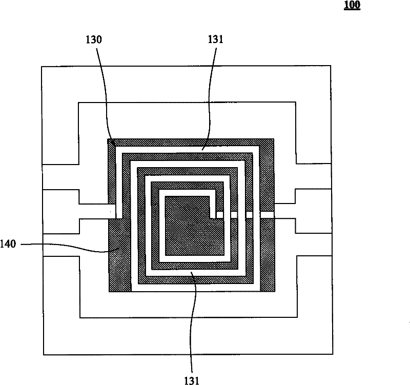
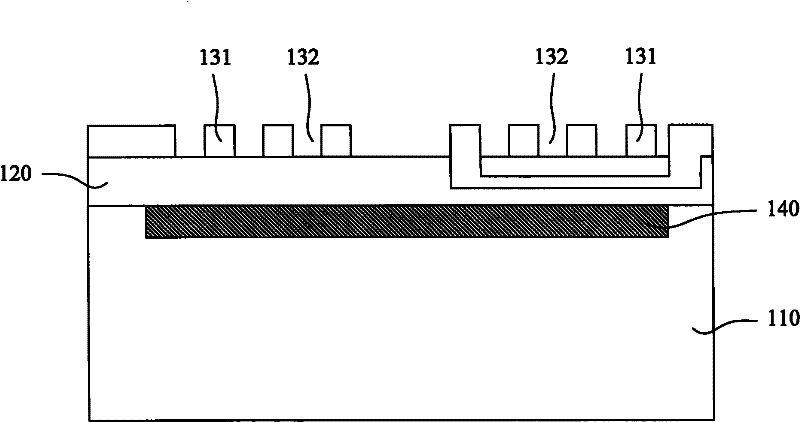
[0031] Please refer to Figure 1A and Figure 1B ,in, Figure 1A It is a top view of the planar spiral inductor provided by Embodiment 1 of the present invention, Figure 1B It is a cross-sectional view of the planar spiral inductor provided by Embodiment 1 of the present invention.
[0032] Such as Figure 1A and Figure 1B As shown, the planar spiral inductor 100 includes: a semiconductor substrate 110, a dielectric layer 120, a planar spiral inductor body 130 and an insulating isolation structure 140, the dielectric layer 120 is formed on the semiconductor substrate 110, and the planar spiral inductor body 130 is formed on the dielectric layer 120 , and the insulating isolation structure 140 is formed in the semiconductor substrate 110 and corresponds to the planar spiral inductor body 130 . Wherein, the planar spiral inductor body 130 includes: multi-turn coils 131 and interval regions 132 between the multi-turn coils 131 , and the multi-turn coils 131 are formed by wind...
Embodiment 2
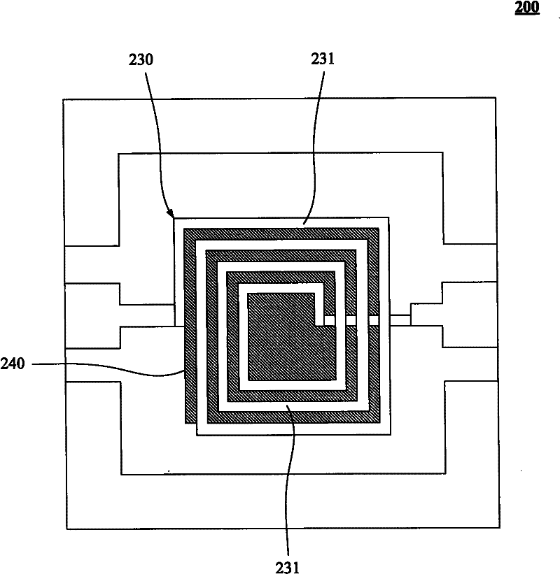
[0045] Please refer to Figure 2A and Figure 2B ,in, Figure 2A It is a top view of the planar spiral inductor provided by Embodiment 2 of the present invention, Figure 2B It is a cross-sectional view of the planar spiral inductor provided by Embodiment 2 of the present invention.
[0046] Such as Figure 2A and Figure 2B As shown, the planar spiral inductor 200 includes: a semiconductor substrate 210, a dielectric layer 220, a planar spiral inductor body 230 and an insulating isolation structure 240, the dielectric layer 220 is formed on the semiconductor substrate 210, and the planar spiral inductor body 230 is formed On the dielectric layer 220 , the isolation structure 240 is formed in the semiconductor substrate 210 and corresponds to the planar spiral inductor body 230 . Wherein, the planar spiral inductor body 230 includes: multi-turn coils 231 and interval regions 232 between the multi-turn coils 231 . The difference between this embodiment and the first embod...
Embodiment 3
[0048] Please refer to image 3 , which is a top view of the planar spiral inductor provided by Embodiment 3 of the present invention. Such as image 3 As shown, the difference between this embodiment and other embodiments is that the insulating isolation structure 340 of the planar spiral inductor 300 is formed in the semiconductor substrate, and the insulating isolation structure 340 is located in the innermost coil area of the multi-turn coil 331 It should be noted that the area inside the innermost coil includes the innermost coil itself, that is, the area of the semiconductor substrate surface below the center of the planar spiral inductor body 330 is completely replaced by insulating materials.
PUM
| Property | Measurement | Unit |
|---|---|---|
| Thickness | aaaaa | aaaaa |
| Thickness | aaaaa | aaaaa |
Abstract
Description
Claims
Application Information
 - R&D
- Intellectual Property
- Life Sciences
- Materials
- Tech Scout
- Unparalleled Data Quality
- Higher Quality Content
- 60% Fewer Hallucinations
Browse by: Latest US Patents, China's latest patents, Technical Efficacy Thesaurus, Application Domain, Technology Topic, Popular Technical Reports.
© 2025 PatSnap. All rights reserved.Legal|Privacy policy|Modern Slavery Act Transparency Statement|Sitemap|About US| Contact US: help@patsnap.com