Silicon-on-insulator (SOI) body contact metal oxide semiconductor (MOS) transistor and forming method thereof

A MOS transistor, body contact technology, applied in semiconductor devices, semiconductor/solid-state device manufacturing, electrical components, etc., can solve problems such as obvious floating body effect, and achieve the effect of improving device performance, suppressing floating body effect, and improving stable performance.

Active Publication Date: 2011-10-05
SHANGHAI HUAHONG GRACE SEMICON MFG CORP
View PDF4 Cites 4 Cited by
  • Summary
  • Abstract
  • Description
  • Claims
  • Application Information

AI Technical Summary

Problems solved by technology

[0005] But when the SOI device is in use, the

Method used


Image

  • Silicon-on-insulator (SOI) body contact metal oxide semiconductor (MOS) transistor and forming method thereof
  • Silicon-on-insulator (SOI) body contact metal oxide semiconductor (MOS) transistor and forming method thereof
  • Silicon-on-insulator (SOI) body contact metal oxide semiconductor (MOS) transistor and forming method thereof

Examples


Embodiment Construction

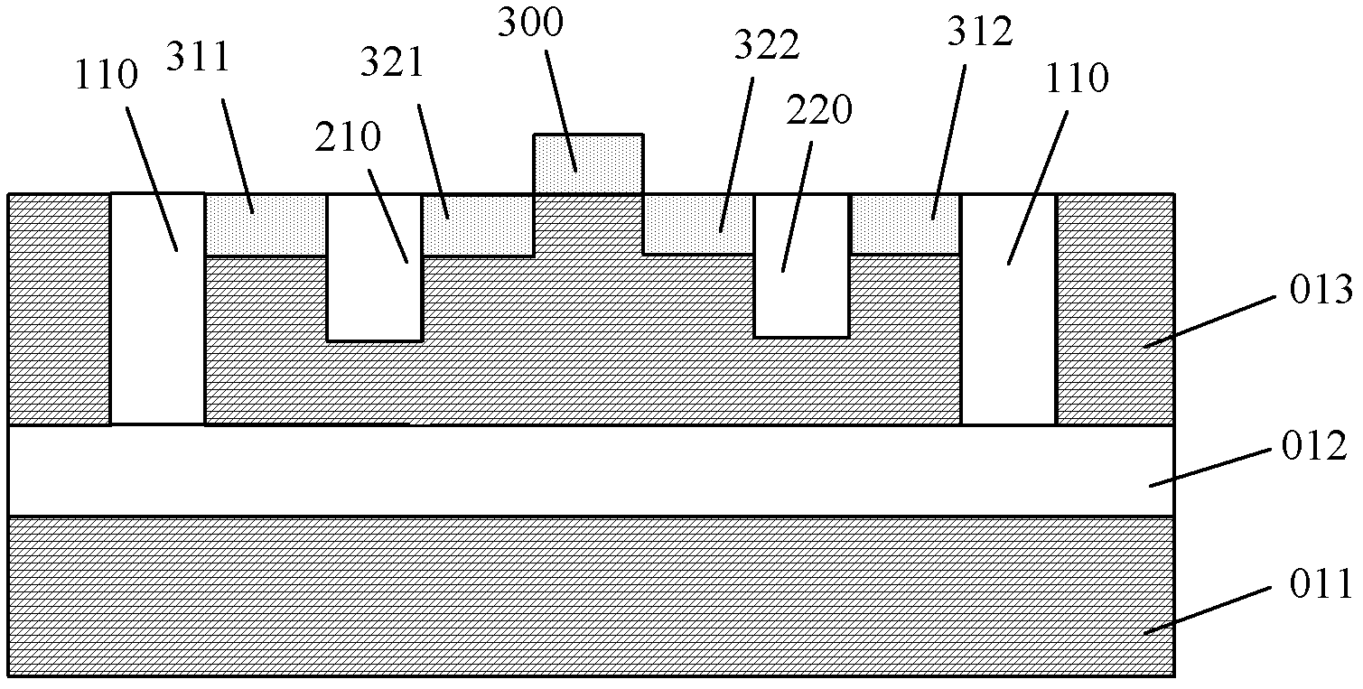
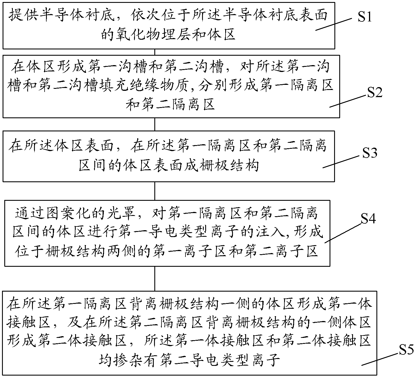
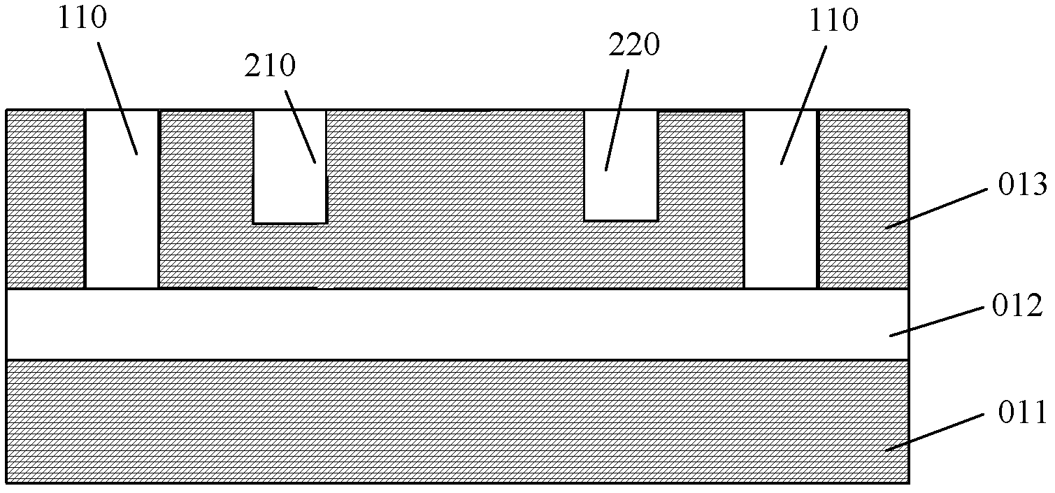
[0034] In the prior art, after the SOI body contact MOS transistor structure is turned on, obvious floating body effects may still appear from time to time, which is mainly manifested in that the floating body effect is obvious after the source and drain terminals of the SOI body contact MOS transistors are exchanged.

[0035] In order to solve the above problems, the present invention provides an SOI body contact MOS transistor, including:

[0036] A semiconductor substrate, the buried oxide layer and the body region on the surface of the semiconductor substrate in turn;

[0037] The gate structure located on the surface of the body region, and the first ion region and the second ion region located in the body regions on both sides of the gate structure, the first ion region and the second ion region are both doped with the first ion region A conductivity type ion;

[0038] It also includes a first body contact region in the body region on the side of the first ion region away from t...


PUM

PropertyMeasurementUnit
Thickness rangeaaaaaaaaaa
Thicknessaaaaaaaaaa
Thicknessaaaaaaaaaa

Abstract

The invention provides a silicon-on-insulator (SOI) body contact metal oxide semiconductor (MOS) transistor, which comprises a semiconductor substrate, an oxide buried layer, a body region, a grid structure, a first ion region, a second ion region, a first body contact region and a second body contact region, wherein the oxide buried layer and the body region are positioned on the surface of the semiconductor substrate in turn; the grid structure is positioned on the surface of the body region; the first ion region and the second ion region are positioned in the body region on two sides of the grid structure; first conductive ions are doped in the first ion region and the second ion region; the first body contact region is positioned in the body region of the first ion region on one side deviated from the grid structure; the second body contact region is positioned in the body region of the second ion region on one side deviated from the grid structure; and second conductive ions are doped in the first body contact region and the second body contact region. The invention also provides a method for forming the SOI body contact MOS transistor. By the SOI body contact MOS transistor and the forming method thereof, a floating body effect can be suppressed, and the device performance is improved.

Description

Technical field [0001] The present invention relates to the technical field of semiconductor manufacturing, in particular to an SOI body contact MOS transistor and a method for forming the same. Background technique [0002] The silicon-on-insulator (SOI) structure has many advantages compared with the conventional bulk silicon substrate, such as: elimination of latch-up effect, reduced short-channel effect of the device, improved resistance to radiation, etc. . Therefore, many semiconductor chip manufacturers use SOI substrates to make MOS transistors. [0003] While the SOI technology brings improvements in device and circuit performance, it also inevitably brings adverse effects. The biggest problem is the floating body effect of partially depleted SOI devices. When the thickness of the silicon film on the top layer of the device is greater than the width of the maximum depletion layer, due to the isolation effect of the buried oxide layer in the structure, a part of the silic...

Claims


Application Information

Patent Timeline
IPC IPC(8): H01L29/78H01L29/06H01L21/336
Inventor 蒙飞仇超
Owner SHANGHAI HUAHONG GRACE SEMICON MFG CORP
Why Eureka
Try Eureka