Film formation substrate, manufacturing method for film formation substrate and film formation device

A manufacturing method and a film-forming technology, which are applied in the direction of final product manufacturing, sustainable manufacturing/processing, ion implantation plating, etc., can solve the problems of increasing waste liquid treatment costs, achieve low cost, reduce film thickness, and do not require Effect of etching process

Inactive Publication Date: 2011-10-05
SUMITOMO HEAVY IND LTD
View PDF5 Cites 0 Cited by
  • Summary
  • Abstract
  • Description
  • Claims
  • Application Information

AI Technical Summary

Problems solved by technology

[0007] In such an etching process, since an etching solution such as hydrochloric acid is used, there is a problem that waste liquid treatment is required and the cost of waste liquid treatment increases.

Method used


Image

  • Film formation substrate, manufacturing method for film formation substrate and film formation device
  • Film formation substrate, manufacturing method for film formation substrate and film formation device
  • Film formation substrate, manufacturing method for film formation substrate and film formation device

Examples


Embodiment Construction

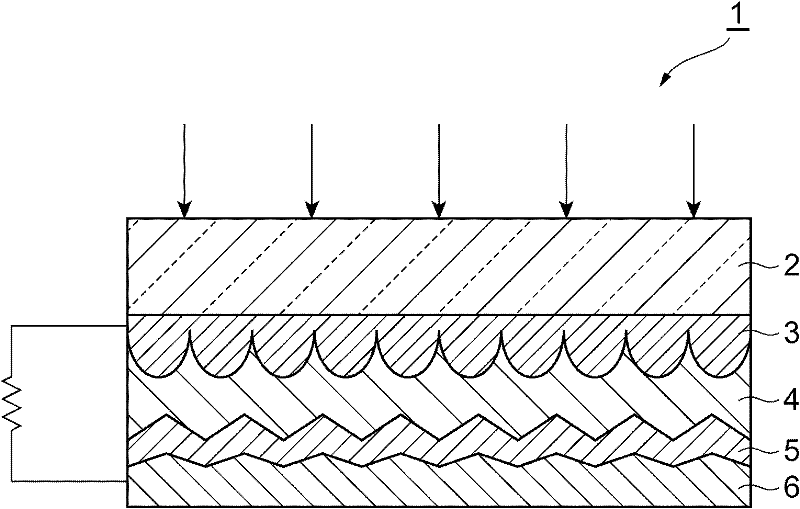
[0025] Hereinafter, best embodiments of a film-forming substrate and a method of manufacturing a film-forming substrate according to the present invention will be described with reference to the drawings. The film-forming substrate of the present invention is used, for example, as a transparent electrode of a solar cell module. figure 1 It is a cross-sectional view of the solar cell module according to the embodiment of the present invention. In addition, in description of drawings, the same code|symbol is attached|subjected to the same or equivalent element, and repeated description is abbreviate|omitted.

[0026] Such as figure 1 The solar cell module 1 shown is an amorphous silicon type solar cell, and a transparent conductive film 3, an amorphous silicon (hereinafter referred to as "a-Si") layer 4, an aluminum zinc oxide (AZO ) layer 5 and Ag electrode 6.

[0027] The glass substrate 2 is disposed on the incident side of light, and corresponds to the film formation subs...


PUM


Abstract

The invention provides a film formation substrate, a manufacturing method for film formation substrate and a film formation device, which are advantaged by not requiring for etching procedure during seeking for reduction of film thickness and seeking for low cost. A thin-film layer provided with a rugged structure is formed on a film formation substrate. The film formation substrate (1) is provided with a rugged-structured thin-film layer (3) formed on a substrate at a flat part on the surface of a film formed substrate (2), and the rugged structure is formed by film forming of the thin-film layer (3) containing indium oxide. Additionally, the manufacturing method for a film formation substrate is a method of manufacturing the rugged-structured thin-film layer (3) in film formation on the substrate (1) at the flat part on the surface of the film formed substrate (2), the manufacturing method is provided with a thin-film procedure, which is characterized in that, the thin-film layer (3) containing indium oxide is formed on the surface of the film formed substrate (2), and the rugged structure is formed via performing of the film formation. Therefore, the etching procedure used for forming the rugged structure is not needed and low cost is sought, and a transparent conductive film (3) containing indium oxide is set to reduce film thickness.

Description

technical field [0001] The present invention relates to a film-forming substrate in which a thin film layer having a concavo-convex structure is formed on a flat portion of the film-forming substrate, a method for manufacturing the film-forming substrate, and a film-forming apparatus. Background technique [0002] For example, in an amorphous silicon type solar cell, a transparent electrode formed with a concavo-convex structure (texture structure) for scattering light incident on the light receiving portion is used. This makes it possible to optimally scatter the light incident on the light receiving unit and confine the light in the solar cell module, thereby making effective use of the incident light and improving power generation efficiency. [0003] In the transparent electrode formed with such a concavo-convex structure, tin oxide (SnO 2 ). Since tin oxide has a high volume resistivity, it is necessary to increase the film thickness in order to realize the surface re...

Claims


Application Information

Patent Timeline
Patent Type & Authority Applications(China)
IPC IPC(8): C23C14/08H01L31/18C23C14/34H01L31/04
CPCY02E10/50Y02P70/50
Inventor 岩田宽
Owner SUMITOMO HEAVY IND LTD
Why Eureka
Try Eureka